|
Troy NY (SPX) Nov 13, 2006 Many of the vaunted applications of carbon nanotubes require the ability to attach these super-tiny cylinders to electrically conductive surfaces, but to date researchers have only been successful in creating high-resistance interfaces between nanotubes and substrates. Now a team from Rensselaer Polytechnic Institute reports two new techniques, each following a different approach, for placing carbon nanotube patterns on metal surfaces of just about any shape and size. The results, which appear in separate papers from the November issue of Nature Nanotechnology and the Oct. 16 issue of Applied Physics Letters (APL), could help overcome some of the key hurdles to using carbon nanotubes in computer chips, displays, sensors, and many other electronic devices. "Carbon nanotubes offer promising applications in fields ranging from electronics to biotechnology," said Saikat Talapatra, a postdoctoral research associate with the Rensselaer Nanotechnology Center and lead author of the Nature Nanotechnology paper. But since many of these applications are based on the superior conductivity of carbon nanotubes, good contact between nanotubes and conducting metal components is essential. Both of the newly developed techniques could bring the use of nanotubes as interconnects on computer chips closer to reality - a long-sought goal in the nanotechnology community. As chip makers seek to continually increase computing power, they are looking to shrink the dimensions of chip components to the nanometer scale, or about 1-100 billionths of a meter. Communication between components becomes increasingly difficult at this incredibly small scale, making carbon nanotubes a natural choice to replace metal wires, according to the researchers. In the first technique - dubbed "floating catalyst chemical vapor deposition" - they heat a carbon-rich compound at extremely high temperatures until the material vaporizes. As the system cools, carbon deposits directly on the metal surface in the form of nanotube arrays. For this experiment, the team used surfaces made from Inconel, a nickel-based "super alloy" with good electrical conductivity. Until now this technique has only been used to grow nanotubes on substrates that are poor conductors of electricity. There are many potential advantages to growing carbon nanotubes directly on metals with this simple, single-step process, according to Talapatra. Nanotubes attach to the surface with much greater strength; excellent electrical contact is established between the two materials; and nanotubes can be grown on surfaces of almost any shape and size, from curved sheets to long metal rods. But chemical vapor deposition is a high-temperature process, which makes it incompatible with some sensitive electronic applications. "We have developed an alternate process of obtaining carbon nanotube arrays on any conducting substrate by contact printing methods," said Ashavani Kumar, a postdoctoral research associate in materials science and engineering at Rensselaer and lead author of the APL paper. In collaboration with Rajashree Baskaran, a staff research engineer in the Components Research Division at Intel Corporation, the team developed a procedure that mimics the way photographs are printed from a film negative. They first grow patterns of carbon nanotubes on silicon surfaces using chemical vapor deposition, and then the nanotubes are transferred to metal surfaces that are coated with solder - a metal alloy that is melted to join metallic surfaces together. The nanotubes stick in the solder, maintaining their original arrangement on the new surface. And since solder has a low melting point, the process takes place at low temperature. "The contact printing process we have developed provides a potentially versatile method of incorporating carbon nanotubes in applications which cannot tolerate the typical high temperature of growth," Baskaran said. In addition to showing promise for interconnects in computer chips, carbon nanotubes also exhibit a physical property called "field emission." When a voltage is applied, electrons are pulled out from the surface, which means that nanotubes could be combined with metals to produce high-resolution electronic displays, chemical sensors, and flash memory devices for computers. The researchers also demonstrated that the chemical vapor deposition procedure can be used to make nanotube electrodes for "super capacitors" - devices that have unusually high energy densities when compared to common capacitors, which are used to store energy in electrical circuits. These are of particular interest in automotive applications for hybrid vehicles and as supplementary storage for battery electric vehicles, according to the researchers. The research published in Nature Nanotechnology was funded by the National Science Foundation and the Interconnect Focus Center. The APL work was funded by Intel Corporation via a gift grant. Both projects were performed under the guidance of Pulickel Ajayan, the Henry Burlage Professor of Materials Science and Engineering at Rensselaer and a world-renowned expert in fabricating nanotube-based materials. Other Rensselaer researchers involved with the project are: Robert Vajtai, Swastik Kar, Omkaram Nalamasu, Victor Pushparaj, Sunil Pal, Lijie Ci, Mancheri Shaijumon, and Sumanjeet Kaur. Community Email This Article Comment On This Article Related Links Rensselaer Polytechnic Institute Nano Technology News From SpaceMart.com Nano Technology News From SpaceMart.com Computer Chip Architecture, Technology and Manufacture
 Ann Arbor MI (SPX) Nov 13, 2006
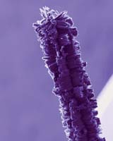
New implantable biomedical devices that can act as artificial nerve cells, control severe pain, or allow otherwise paralyzed muscles to be moved might one day be possible thanks to developments in materials science. Writing today in Advanced Materials, Nicholas Kotov of the University of Michigan, USA, and colleagues describe how they have used hollow, submicroscopic strands of carbon, carbon nanotubes, to connect an integrated circuit to nerve cells. |
|
| The content herein, unless otherwise known to be public domain, are Copyright 1995-2006 - SpaceDaily.AFP and UPI Wire Stories are copyright Agence France-Presse and United Press International. ESA PortalReports are copyright European Space Agency. All NASA sourced material is public domain. Additionalcopyrights may apply in whole or part to other bona fide parties. Advertising does not imply endorsement,agreement or approval of any opinions, statements or information provided by SpaceDaily on any Web page published or hosted by SpaceDaily. Privacy Statement |