|
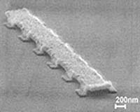
Davis CA (SPX) Apr 11, 2005 They look like an elegant row of columns, tiny enough for atomic-scale hide-and-seek, but these colonnades represent a new way to bring nanotechnology into mass production. Nanotechnology, the ability to create and work with structures and materials on an atomic scale, holds the promise of extreme miniaturization for electronics, chemical sensors and medical devices. But while researchers have created tiny silicon wires and connected them together one at a time, these methods cannot easily be scaled up. "It takes weeks to make one or two, and you end up with different sizes and characteristics," said M. Saif Islam, assistant professor of electrical and computer engineering, who joined UC Davis from Hewlett-Packard Laboratories in 2004. Like handmade shoes, every manually assembled nanostructure comes out slightly different. Engineers would rather build devices the way cars or computers are built, with every item as consistent as possible. While working at the Quantum Science Research group of Hewlett-Packard Laboratories, Islam and colleagues came up with a new approach. Silicon wafers used for building microcircuits are usually polished at one specific angle to the atomic planes of silicon. Instead, the group used a wafer that was polished at a different angle, changing the orientation of silicon atomic planes to the surface. Using a chemical vapor deposition technique, they could then grow identical, perpendicular columns of silicon. The researchers have used this method to grow "nanobridges" across a gap between two vertical silicon electrodes. The nanobridges are strong, chemically stable and show better electrical properties than previous approaches, Islam said. They could be used for nanosized transistors, chemical sensors or lasers. Taking the approach a step further, Islam and his colleagues at Hewlett-Packard made sandwiches of silicon and insulator and partly etched away the top layer to create awning-shaped structures of silicon supported by insulator. Silicon columns grown under the awnings form miniature colonnades. The method allows engineers to combine nanowires of precise length with other silicon structures such as integrated circuits, he said. At UC Davis, Islam plans to continue work on converting the technology into practical devices. The "nanobridge" technique was reported most recently in the March 2005 issue of the journal Applied Physics Part A. The nanocolonnade work was presented April 1 at the spring meeting of the Materials Research Society in San Francisco. Community Email This Article Comment On This Article Related Links UC Davis SpaceDaily Search SpaceDaily Subscribe To SpaceDaily Express Nano Technology News From SpaceMart.com Computer Chip Architecture, Technology and Manufacture
 Houston TX (SPX) Oct 05, 2005
Using a method for assessing the premiums that companies pay for insurance, a team of scientists and insurance experts have concluded that the manufacturing processes for five, near-market nanomaterials - including quantum dots, carbon nanotubes and buckyballs - present fewer risks to the environment than some common industrial processes like oil refining. |
|
| The content herein, unless otherwise known to be public domain, are Copyright 1995-2006 - SpaceDaily.AFP and UPI Wire Stories are copyright Agence France-Presse and United Press International. ESA PortalReports are copyright European Space Agency. All NASA sourced material is public domain. Additionalcopyrights may apply in whole or part to other bona fide parties. Advertising does not imply endorsement,agreement or approval of any opinions, statements or information provided by SpaceDaily on any Web page published or hosted by SpaceDaily. Privacy Statement |