|
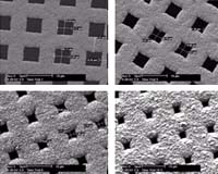
Ann Arbor Mich - Apr 21, 2004 Think of a microscopic milling machine, capable of cutting just about any material with better-than-laser precision, in 3-D---and at the nanometer scale. In a paper published this week in the Proceedings of the National Academy of Sciences, University of Michigan researchers explain how and why using a femtosecond pulsed laser enables extraordinarily precise nanomachining. The capabilities of the ultra-fast or ultra-short pulsed laser have significant implications for basic scientific research, and for practical applications in the nanotechnology industry. Initially, the researchers working at the Center for Ultrafast Optical Science wanted to use the ultra-fast laser as a powerful tool to study structures within living cells, said Alan Hunt, assistant professor, Department of Biomedical Engineering. "It turned out we could push much farther than expected and the applications became broad, from microelectronics applications to MEMS (microelectromechanical systems) to microfluidics," Hunt said. One of the most perplexing problems in nanotechnology is finding an efficient and precise way to build and machine the tiny devices. For example, a human hair is about 100,000 nanometers across. The unique physics of an ultra-short pulsed laser used at a very high intensity make it possible to selectively ablate or cut away features as small as 20 nanometers, Hunt said. This is possible because of the unique physics of how extremely short pulses of light interact with matter; specifically using femtosecond pulses, a blast of light just a quadrillionth of a second long. Currently, there is no easy way to machine a wide variety of materials on the nanometer scale, Hunt said, and the technique with capabilities closest to the ultrafast laser is electron beam lithography. Even this approach does not allow machining below the surface or within a material. Photolithography, the technique used to make computer chips, is used to do such machining on a larger scale but is difficult to get to the nanometer scale, requires specific materials and can generally only be used on one plane. For example, that means that channels on a chip cannot cross without mixing, placing a severe constraint on the microfluidics and "lab on a chip" designs. But the unique physics of the femtosecond pulse allows machining in 3-D, Hunt said. "If we have three channels on a plane, we can link the outer two without cutting into the center one, we can go down over and up, we can cut a U-shape," Hunt said. "Not being constrained to one plane, the level of complexity that can be achieved is much greater." The research team included Hunt; Gerard Mourou, professor of electrical engineering and computer science; Ajit Joglekar, who recently completed his doctorate in biomedical engineering; Hsiao-hua Liu, a post doc at the Center for Ultrafast Optical Science; and Edgar Meyhofer, associate professor of biomedical engineering and mechanical engineering. Community Email This Article Comment On This Article Related Links University of Michigan SpaceDaily Search SpaceDaily Subscribe To SpaceDaily Express Nano Technology News From SpaceMart.com Computer Chip Architecture, Technology and Manufacture
 New York (UPI) Mar 18, 2005
One of the single biggest applications of nanotechnology could be solving the global shortage of pure water, experts told UPI's Nano World. |
|
| The content herein, unless otherwise known to be public domain, are Copyright 1995-2006 - SpaceDaily.AFP and UPI Wire Stories are copyright Agence France-Presse and United Press International. ESA PortalReports are copyright European Space Agency. All NASA sourced material is public domain. Additionalcopyrights may apply in whole or part to other bona fide parties. Advertising does not imply endorsement,agreement or approval of any opinions, statements or information provided by SpaceDaily on any Web page published or hosted by SpaceDaily. Privacy Statement |