|
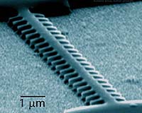
Evanston IL (SPX) Aug 11, 2005 Since the invention of the atomic force microscope (AFM) in 1986 by Nobel laureate Gerd Binnig, the tool has been employed to advance the science of materials in many ways, from nanopatterning (dip-pen nanolithography) to the imaging of surfaces and nano-objects such as carbon nanotubes, DNA, proteins and cells. In all these applications, the quality and integrity of the tip used to obtain the images or interrogate materials is paramount. A common problem in atomic force microscopy is the deterioration of the tip apex as surfaces are scanned. To overcome this problem, a team of scientists from Northwestern University and Argonne National Laboratory report the microfabrication of monolithic ultra-nano-crystalline diamond (UNCD) cantilevers with tips exhibiting properties similar to single-crystal diamond. Their results are published in the Aug. 9 issue of Small, a journal dedicated to breakthroughs in nanoscience and engineering. Diamond, the hardest known material, is probably the optimal tip material for many applications. In addition to hardness, diamond is stiff, biocompatible and wear resistant. Until now, commercially available diamond AFM tips are either glued to a microcantilever (a very slow and non-scalable manufacturing approach) or made by coating a silicon tip manufactured using conventional microfabrication techniques. Chemical vapor deposition (CVD) techniques for growing thin films of synthetic diamond typically do not produce single-crystal films, in which atoms are all oriented in a regular lattice. UNCD, a material discovered at Argonne in the 1990s, is the closest diamond atomic structure in which the material is organized in very small grains (a few nanometers in size) leading to smooth surfaces easy to mold and shape by microfabrication techniques. The similarity of UNCD to single-crystal diamond and its superiority to silicon, silicon carbide and other micro- and nanoelectromechanical systems (MEMS and NEMS) materials, in the context of strength, toughness and wear performance, has been established. The standard MEMS microfabrication techniques used for the diamond tips - an important feature of this development - provides scalability to massively parallel arrays of probes for high throughput. "This technology offers tremendous potential for the large-scale production of single- and two-dimensional tip arrays of doped and undoped diamond exhibiting superior wear resistance and functionality," said team leader, Horacio D. Espinosa, professor of mechanical engineering at Northwestern's McCormick School of Engineering and Applied Science. "The approach can be easily integrated with the AFM Nanofountain Probe (NFP) recently developed by our group and, in this way, achieve the merging of two unique technologies. "The demonstrated low wear and writing capability of UNCD tips with chemical inks is very promising. Moreover, the possibility of doping the material to make it conductive is very exciting and opens a large number of opportunities for scientific discovery. We believe the processing technology will likely lead to many novel applications not only in AFM tips but also in MEMS and NEMS." Potential products range from single UNCD AFM tips for use in commercial AFMs to massively parallel probe systems for high-throughput scanning and nanoscale manufacture. The technology can be employed for a variety of AFM scanning modes, from regular surface scanning in air or fluids to conductive AFM. It can also be employed as a nanofabrication tool. Examples include nanolithography (inorganic ink dispensing), detecting and repairing failure of micro- and nano- electronic devices, nanopatterning of biomolecules (for sequencing, synthesis and drug discovery) and scanning probe electrochemistry (scanning electrode imaging, localized electrochemical etching or deposition of materials and nanovoltametry). Potential markets include those industries where it is pivotal to preserve the performance of the tips or that require two-dimensional arrays for high throughput in which the cost of manufacturing is such that minimum possible tip wear is paramount. Examples include the microelectronics industry (novel random-access memories based on AFM technology, such as IBM's Millipede), the semiconductor industry (photomask repair) and the chemical and biological sensor industry where high throughput and spatial resolution are important. Northwestern is seeking a licensing partner to commercialize the microfabrication processes and methods to produce arrays of the device. A patent application has been filed by the University. In addition to Espinosa, other authors on the Small paper are graduate student Keun-Ho Kim and research assistant professor Nicolaie A. Moldovan from Northwestern and post-doctoral fellow Xingcheng Xiao and research scientists John Carlisle and Orlando Auciello from Argonne National Laboratory (ANL). This research has been supported in part by the National Science Foundation through two initiatives: Nanoscale Interdisciplinary Research Team Award No. CMS00304472 and Nanoscale Science and Engineering Center Award No. EEC�0118025. The ANL team effort has been supported by the Department of Energy's Office of Science under Award No. W-31-109-ENG-38. Community Email This Article Comment On This Article Related Links SpaceDaily Search SpaceDaily Subscribe To SpaceDaily Express Nano Technology News From SpaceMart.com Computer Chip Architecture, Technology and Manufacture
 Newark DE (SPX) Oct 14, 2005
University of Delaware researchers are opening a new front in the war on cancer, bringing to bear new nanotechnologies for cancer detection and treatment and introducing a unique nanobomb that can literally blow up breast cancer tumors. |
|
| The content herein, unless otherwise known to be public domain, are Copyright 1995-2006 - SpaceDaily.AFP and UPI Wire Stories are copyright Agence France-Presse and United Press International. ESA PortalReports are copyright European Space Agency. All NASA sourced material is public domain. Additionalcopyrights may apply in whole or part to other bona fide parties. Advertising does not imply endorsement,agreement or approval of any opinions, statements or information provided by SpaceDaily on any Web page published or hosted by SpaceDaily. Privacy Statement |