|
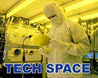
Petaluma CA - Apr 20, 2004 Tegal Corporation, a designer and manufacturer of plasma etch and deposition systems, and Sharp Laboratories of America have entered into an agreement to collaborate on a focused joint development program (JDP) to accelerate the adoption and integration of next generation high-K dielectrics. The JDP builds on Tegal's patented Nano Layer Deposition (NLD) technology for depositing ultra thin layers of new dielectric materials for semiconductor and nanotechnology device production. The program will be centered at the Sharp Laboratories of America (SLA) facility in Camas, Washington and will utilize the Tegal Simplus(TM) NLD system already installed there. "We are very excited about the JDP and the opportunity for Tegal to work cooperatively with Sharp engineers within their own facilities to further refine and deploy production solutions based on Tegal's Simplus NLD technology," said Michael L. Parodi, Tegal's Chairman, President and CEO. "NLD holds the promise of enabling high throughput deposition of critical dielectric layers needed for semiconductor device scaling. The scaling of logic and memory devices requires the continuous thickness reduction of dielectric layers to ensure the required electrical performance of these devices. "New conformal deposition technologies like NLD are needed to achieve the aggressive scaling requirements called out in the recently published Semiconductor Industry Association's (SIA) International Technology Roadmap for Semiconductors (2003)." The Simplus NLD cluster tool is a multi-chamber deposition platform targeted for barrier, copper seed and high-K dielectric applications. The market for highly conformal deposition tools, such as NLD and Atomic Layer Deposition (ALD), is expected to grow from approximately $100 million today to over $1.3 billion by 2008 according to the independent market research firm VLSI Research, Inc. Tegal announced the completion of the acquisition of the Simplus NLD product line in December 2003. Community Email This Article Comment On This Article Related Links Tegal SpaceDaily Search SpaceDaily Subscribe To SpaceDaily Express Nano Technology News From SpaceMart.com Computer Chip Architecture, Technology and Manufacture
 New York (UPI) Mar 18, 2005
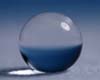
One of the single biggest applications of nanotechnology could be solving the global shortage of pure water, experts told UPI's Nano World. |
|
| The content herein, unless otherwise known to be public domain, are Copyright 1995-2006 - SpaceDaily.AFP and UPI Wire Stories are copyright Agence France-Presse and United Press International. ESA PortalReports are copyright European Space Agency. All NASA sourced material is public domain. Additionalcopyrights may apply in whole or part to other bona fide parties. Advertising does not imply endorsement,agreement or approval of any opinions, statements or information provided by SpaceDaily on any Web page published or hosted by SpaceDaily. Privacy Statement |