|
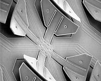
Washington - Jul 29, 2003 When a car collides with another car, a tiny device called an accelerometer detects the change in motion and sets off an air bag, an innovation that has saved many lives. The accelerometer is one of the most common uses of microelectromechanical systems (MEMS), but scientists and engineers also are starting to use them in devices ranging from angioplasty pressure sensors and pacemakers to optical disk drives. MEMS, also known as micromachines, are a relatively new technology that uses existing microelectronics manufacturing methods to create complex machines with micrometer feature sizes. MEMS devices represent a rapidly growing component of the semiconductor industry. Many micromachines contain moving parts that are combined with integrated circuits. Like most high-tech devices, they must be made with precise dimensions and materials properties to operate properly. To help manufacturers ensure that their devices meet these exacting specifications, National Institute of Standards and Technology (NIST) scientists and engineers helped develop three ASTM International standard test methods for the thin films used to make micromachines. The test procedures, which are the first such standards in the world, will be published in The Annual Book of ASTM International Standards this month. The standards are expected to facilitate global commerce in MEMS technologies by enabling measurements that will lead to the development of more reliable and reproducible MEMS devices. The three standards provide detailed instructions for measuring thin-film dimensions and "strain," a property related to the stress in the thin film. NIST researchers have created a Web site to help semiconductor manufacturers perform the complex mathematical calculations required by the new standard test methods. Community Email This Article Comment On This Article Related Links Related Information at NIST SpaceDaily Search SpaceDaily Subscribe To SpaceDaily Express Nano Technology News From SpaceMart.com Computer Chip Architecture, Technology and Manufacture
 New York (UPI) Mar 18, 2005
One of the single biggest applications of nanotechnology could be solving the global shortage of pure water, experts told UPI's Nano World. |
|
| The content herein, unless otherwise known to be public domain, are Copyright 1995-2006 - SpaceDaily.AFP and UPI Wire Stories are copyright Agence France-Presse and United Press International. ESA PortalReports are copyright European Space Agency. All NASA sourced material is public domain. Additionalcopyrights may apply in whole or part to other bona fide parties. Advertising does not imply endorsement,agreement or approval of any opinions, statements or information provided by SpaceDaily on any Web page published or hosted by SpaceDaily. Privacy Statement |