|
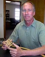
95th Air Base Wing Public Affairs Kirtland AFB NM (AFNS) Jun 06, 2006 About the size of a U.S. quarter, the field programmable gate array computer chip consists of 400 to 500 million transistors and two to three miles of wiring, but its flexible capacity significantly contributed to the Air Force's decision to employ the small component in its next generation of satellite systems. Managed by the Air Force Research Laboratory's Space Vehicles Directorate, Kirtland Air Force Base, N.M., the service's Field Programmable Gate Array Program originated 10 years ago when the initial radiation-hardened version, to protect the semiconductor part from the hazards of cosmos environment, had been designed and developed for use in NASA's Mars Pathfinder mission in 1997. "Since the Mars Pathfinder mission, there has been a one thousand-fold increase in the amount of data that is transmitted, and that trend will continue in the future," said Creigh Gordon, Field Programmable Gate Array program manager, Air Force Research Laboratory's Space Vehicles Directorate. "That is motivation enough for our program to advance a new field programmable gate array computer chip to meet the increasing demand of new technology," he noted. Invented in the commercial sector in the mid-1980s, the field programmable gate array computer chip differs from a standard microprocessor, which serves a specific purpose such as image compression or video streaming, because the same device can be reprogrammed to perform multiple functions. Transformation of the chip, however, comes with an initial, upfront price tag of between $10 and $20 million, with successive manufactured copies costing considerably less at a few cents apiece. Nevertheless, for its first Field Programmable Gate Array program venture with NASA in 1996, funded by the Department of Energy and Sandia National Laboratories, the program contracted with Actel Corp., Mountain View, Calif., to deliver a product, modified for radiation hardening, for the historic, premier mission to the red planet. Following that success, the technology transferred to the private sector, and since then, over 250,000 of the miniature microprocessors have been produced. "The field programmable gate array computer chip provided for NASA in 1996 featured an 8,000 logic gate capacity," said Gordon. "For our current project, the chip will consist of between one to two million logic gates," explained the senior electronics engineer. "The chip's capacity has doubled every year and, in addition, has gotten more complex." Last year, Gordon began working to secure a new field programmable gate array computer chip for employment in Air Force spacecraft in the next two to three years. With $15 to $20 million support from the Missile Defense Agency, the Air Force's Space and Missile Systems Center, NASA and Air Force Research Laboratory, the program is working with XILINX, San Jose, Calif., and again with Actel Corp., to design, develop, and manufacture the latest radiation hardened adaptation. Like its predecessor in the previous decade, the new and improved computer chip will eventually transition to the commercial market. "Our program's objective is to take commercially available electronic technology and modify it for military requirements," Gordon pointed out. "We are on track technically to meet the Air Force's need of applying the latest radiation-hardened field programmable gate array computer chip in the next generation of space vehicles," he said. "Of course, with the unbelievable rate of technology change occurring daily, the field programmable gate array computer chip will likely get even smaller, but will pack plenty of power." Community Email This Article Comment On This Article Related Links Air Force Research Laboratory Computer Chip Architecture, Technology and Manufacture Nano Technology News From SpaceMart.com
 Greenbelt MD (SPX) May 25, 2006
An inexpensive detector developed by a NASA-led team can now see invisible infrared light in a range of "colors," or wavelengths. The detector, called a Quantum Well Infrared Photodetector (QWIP) array, was the world's largest (one million-pixel) infrared array when the project was announced in March 2003. |
|
| The content herein, unless otherwise known to be public domain, are Copyright 1995-2006 - SpaceDaily.AFP and UPI Wire Stories are copyright Agence France-Presse and United Press International. ESA PortalReports are copyright European Space Agency. All NASA sourced material is public domain. Additionalcopyrights may apply in whole or part to other bona fide parties. Advertising does not imply endorsement,agreement or approval of any opinions, statements or information provided by SpaceDaily on any Web page published or hosted by SpaceDaily. Privacy Statement |