|
San Jose - Nov 19, 2002 The future of nanoelectronics looks promising. Built with nanotubes and various self-assembling molecular structures, this technology may revolutionize the electronic world by replacing the silicon transistor in approximately ten years. Chemically synthesized nano building blocks are expected to replace semiconductor logic and memory devices and target niche applications over the next decade. "In 20 to 50 years, we will likely see wide-ranging use of self-assembly," says Technical Insights Director of Research Leo O'Connor. Extreme ultraviolet (EUV) lithography is currently favored by chipmakers, and some companies are expected to use EUV to replace 157 nm scanners in the second half of the decade. Japanese electronic companies have joined forces to develop low-energy electron-beam proximity projection lithography. Currently, chipmakers are working to make the 157 nm lithography technology operational by 2003. In doing so, they have come up against many obstacles such as the availability of calcium fluoride for lens manufacturing and contamination of optical elements. Researchers are working to address these difficulties. Recently, supporters of various forms of next-generation lithography reported progress on 157 nm optical, projection e-beam lithography and EUV lithography. Although expensive, EUV scanners will work at the 13.5 nm wavelength and take manufacturers over several process generations. Although chip technology plays a crucial role in the semiconductor industry, researchers believe that it is only a matter of time before the switch from lithographed silicon chips to self-assembled nanoelectronics takes place. In anticipation of the eventual change, researchers at various universities are experimenting with different technologies. At Delft University in the Netherlands, for example, researchers have built basic logic circuits with carbon nanotubes, while at Harvard University a group of researchers used indium phosphide nanowires to build the same types of devices. Molecular self-assembly is not without its share of problems. Despite challenges, it seems clear that nanotechnology will have a profound impact on the future development of many sectors, particularly that of electronics, which demands technologies that enable faster processing of data at lower costs. Community Email This Article Comment On This Article Related Links Technical-Insights At Frost & Sullivan SpaceDaily Search SpaceDaily Subscribe To SpaceDaily Express Nano Technology News From SpaceMart.com Computer Chip Architecture, Technology and Manufacture
 New York (UPI) Mar 18, 2005
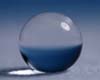
One of the single biggest applications of nanotechnology could be solving the global shortage of pure water, experts told UPI's Nano World. |
|
| The content herein, unless otherwise known to be public domain, are Copyright 1995-2006 - SpaceDaily.AFP and UPI Wire Stories are copyright Agence France-Presse and United Press International. ESA PortalReports are copyright European Space Agency. All NASA sourced material is public domain. Additionalcopyrights may apply in whole or part to other bona fide parties. Advertising does not imply endorsement,agreement or approval of any opinions, statements or information provided by SpaceDaily on any Web page published or hosted by SpaceDaily. Privacy Statement |