|
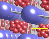
Arlington - Jun 30, 2003 Scientists from Columbia University, IBM and the University of New Orleans today announced a new, three-dimensional designer material assembled from two different types of particles only billionths of a meter across. In the June 26 issue of the journal Nature, the team describes the precision chemistry methods developed to tune the particles' sizes in increments of less than one nanometer and to tailor the experimental conditions so the particles would assemble themselves into repeating 3-D patterns. The work was supported in part by the National Science Foundation, the independent agency that supports basic research in all fields of science and engineering, through the Center for Nanostructured Materials at Columbia University and by the Defense Advanced Research Agency (DARPA) through programs on metamaterials and advanced thermoelectric materials. Designing new materials with otherwise unattainable properties, sometimes referred to as "metamaterials," is one of the promises of nanotechnology. Two-dimensional patterns had previously been created from gold nanoparticles of different sizes and mixtures of gold and silver. Extending this concept to three dimensions with more diverse types of materials demonstrates the ability to bring more materials together than previously realized. "What excites us the most is that this is a modular assembly method that will let us bring almost any materials together," said Christopher Murray, manager of nanoscale materials and devices at IBM Research. "We've demonstrated the ability to bring together complementary materials with an eye to creating materials with interesting custom properties." Murray worked with Stephen O'Brien, assistant professor of applied physics and applied mathematics at Columbia University; Franz Redl, a postdoctoral researcher affiliated with both Columbia and IBM; and Kyung Sang Cho, a post-doctoral researcher affiliated with IBM and supported by the Advanced Materials Research Institute of the University of New Orleans. The scientists chose the materials for the experiments specifically because of their dissimilar, yet complementary properties. Lead selenide is a semiconductor that has applications in infrared detectors and thermal imaging and can be tuned to be more sensitive to specific infrared wavelengths. The other material, magnetic iron oxide, is best known for its use in the coatings for certain magnetic recording media. The combination of these nanoparticles may have novel magneto-optical properties as well as properties key to the realization of quantum computing. For example, it might be possible to modulate the material's optical properties by applying an external magnetic field. "This was a demonstration of the ability to create such materials," O'Brien said. "Given the unique combination of these nanoscale materials, we're in uncharted territory with respect to the properties, which we will be working on in the future." The first step was to create the nanoparticles. The particle sizes were calculated from the mathematical ideal of the structures they wanted to create. In addition to fine-tuning the sizes, the particles had to be very uniform, all within 5 percent of the target size. They settled on iron oxide particles 11 nanometers in diameter, which were created by Redl, and lead selenide particles 6 nanometers in diameter, created by Cho. There are approximately 60,000 atoms in one of the iron oxide nanoparticles and approximately 3,000 atoms in the lead selenide particles. Next, Redl assembled the nanoparticles--or more to the point, had the particles assemble themselves--into three different repeating 3-D patterns by tailoring the experimental conditions. Forming these so-called "crystal structures," as opposed to random mixtures of nanoparticles, is essential for the composite material to exhibit consistent, predictable behaviors. Various other materials are known to assemble spontaneously into these structures of close-packed particles, but none has been made of two components in three dimensions and at the length scales reported in the Nature paper. "The precise and energy-efficient self-assembly of matter into material structures with properties that cannot be achieved otherwise is an important goal for nanotechnology," said Mihail Roco, NSF senior advisor for nanotechnology and chair of the National Science and Technology Council's Subcommittee on Nanoscale Science and Engineering. "This is just one way that nanotechnology will help foster 'the next industrial revolution.'" Community Email This Article Comment On This Article Related Links National Science Foundation SpaceDaily Search SpaceDaily Subscribe To SpaceDaily Express Nano Technology News From SpaceMart.com Computer Chip Architecture, Technology and Manufacture
 New York (UPI) Mar 18, 2005
One of the single biggest applications of nanotechnology could be solving the global shortage of pure water, experts told UPI's Nano World. |
|
| The content herein, unless otherwise known to be public domain, are Copyright 1995-2006 - SpaceDaily.AFP and UPI Wire Stories are copyright Agence France-Presse and United Press International. ESA PortalReports are copyright European Space Agency. All NASA sourced material is public domain. Additionalcopyrights may apply in whole or part to other bona fide parties. Advertising does not imply endorsement,agreement or approval of any opinions, statements or information provided by SpaceDaily on any Web page published or hosted by SpaceDaily. Privacy Statement |