|
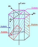
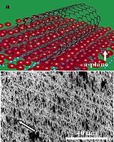
Los Angeles CA (SPX) Apr 26, 2005 On crystal surfaces, nanotubes self-guide themselves into dense structures with exciting potential applications as sensors or integrated circuits USC researchers have found that sapphire surfaces spontaneously arrange carbon nanotubes into useful patterns - but only the right surfaces. Nanotubes are one-atom thick sheets of carbon rolled into seamless cylinders. They can be used to work as chemical sensors and transistors, like devices made from carbon's close chemical cousin, silicon. As a substrate for the creation of single wall nanotube (SWNT) devices, sapphire has a critical advantage, says Chongwu Zhou of the USC Viterbi School of Engineering's department of electrical engineering. Single walled carbon nanotubes will grow along certain crystalline orientations on sapphire. No template has to be provided to guide this structuring: it takes place automatically. Or more accurately, it sometimes happens automatically. With an elegant experiment, Zhou has resolved how and why this occurs. The process is potentially predictable and controllable, opening the door for systematic exploration of sapphire as a SWNT (single wall nanotube) transistor medium. In a paper accepted by the Journal of the American Chemical Society (V127, P5294, 2005), Zhou says the understanding "may allow registration-free fabrication and integration of nanotube devices by simply patterning source/ drain electrodes at desired locations, as the active material (i.e., nanotubes) is all over the substrate," to build such devices as sensors and integrated circuits for various uses. According to Zhou, nanotube transistor devices now have to be painstakingly positioned and aligned using methods such as flow alignment and electrical-field-assisted alignment and then individually connected.
|