|
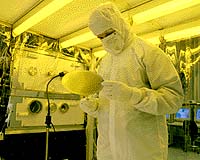
Geneva (SPX) Jul 08, 2004 STMicroelectronics, one of the world's leading semiconductor suppliers, has announced significant progress in the development of a new type of electronic memory that could eventually replace the Flash memory technology. Today, Flash is a key component of many electronic applications, from mobile phones, digital cameras, and set-top boxes to automotive engine controllers. The new technology, called Phase-Change Memory (PCM), potentially offers better performance than Flash. Most importantly, PCM is better suited to continuing the rapid shrinking of features for cost and speed advantage that has long characterized the semiconductor industry than Flash and other so-called "Non-Volatile Memories" (NVM), which are able to store information even when their power is switched off. Even though the market for Flash memories today is very large and is currently one of the fastest growing sectors of the semiconductor market, chip manufacturers have known for many years that it will become increasingly difficult to keep on reducing the size of the basic Flash memory cell. The continual reduction of cell size is essential to electronics equipment manufacturers because it makes the electronic memories and the equipment that relies on them cheaper, thereby stimulating market growth. In the ten years from 1990 to 2000, the size of an individual Flash cell was reduced by a factor of 30 and chip manufacturers are confident that they can continue developing innovative new Flash products for at least another ten years before they will face increasingly difficult challenges to overcome fundamental physical limits. For this reason, all Flash memory manufacturers have been investigating candidate technologies for the "post-Flash" era. Three years ago, ST concluded that the Phase-Change Memory technology, developed by California-based Ovonyx, Inc and already used in re-writable CDs, could be adapted as a semiconductor memory technology. In 2001, ST licensed the technology, also known as Ovonic Unified Memory, from Ovonyx and the two companies set up a joint-development team, largely based in Agrate Brianza, near Milan, where ST's worldwide NVM development is centred. The new memory technology exploits the fact that certain so-called 'chalcogenide' materials can be reversibly switched between two stable states - one amorphous with a high electrical resistance, the other crystalline with a low resistance - by appropriately heating the material. A memory cell in the new technology consists essentially of a variable resistance formed by the chalcogenide material and its tiny electrical heater, along with a selection transistor used for the read/write operations. ST's progress towards developing a commercial PCM technology was described in two papers presented at one of the semiconductor industry's most important annual forums, the VLSI Technology and Circuits Symposia held in Honolulu on June 15-19, 2004. In one paper, ST showed for the first time an innovative cell structure that can be easily integrated into the mainstream chip manufacturing process and which gives good indications of its manufacturability and cost. In a second paper, ST described the practical implementation of this technology in the form of an 8-Mbit demonstrator chip designed to assess the feasibility of cost-effective large non-volatile memories. Based on the highly-promising results it has obtained to date, ST already envisages the new Phase-Change Memory technology being used in medium-density, stand-alone memories and embedded applications. Moreover, by demonstrating the feasibility of the key features that make the PCM cell most attractive, ST has increased its confidence in the long-term scalability of the technology, which will eventually allow PCM to become a mainstream Non-Volatile Memory technology. Community Email This Article Comment On This Article Related Links STMicroelectronics SpaceDaily Search SpaceDaily Subscribe To SpaceDaily Express Space Technology News - Applications and Research
 Baltimore MD (SPX) Jan 12, 2006
A team comprised of three leading US aerospace and defense contractors has demonstrated an innovative technological use of active electronically scanned array (AESA) radars for high-bandwidth communications. |
|
| The content herein, unless otherwise known to be public domain, are Copyright 1995-2006 - SpaceDaily.AFP and UPI Wire Stories are copyright Agence France-Presse and United Press International. ESA PortalReports are copyright European Space Agency. All NASA sourced material is public domain. Additionalcopyrights may apply in whole or part to other bona fide parties. Advertising does not imply endorsement,agreement or approval of any opinions, statements or information provided by SpaceDaily on any Web page published or hosted by SpaceDaily. Privacy Statement |