|
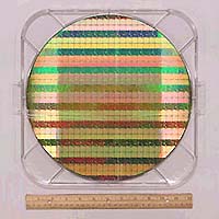
New York NY (SPX) Nov 10, 2004 Albany Nanotech and Advanced Micro Devices have entered into a joint R&D project to develop a new nanometrology capability for measuring the stress state in strained silicon, a material at the heart of high-performance microchips. "Straining," or stretching, silicon speeds the flow of electrons through transistors, increasing the performance of semiconductors and decreasing power consumption. The new technique seeks to enable the stress state in strained silicon to be measured with a target spatial resolution better than 10 nanometers (nm), a critical capability for controlling and improving the performance in semiconductor integrated circuits. The project will focus on near-field nano-optical techniques, exploiting the enhancement of the optical field at a nanoprobe tip. This new technique would facilitate more accurate measurements, helping to enable chip manufacturers to reduce costs as well as time to market for leading-edge microprocessors. AMD chose Albany Nanotech as the headquarters for this research due to its on-site scientists' extensive experience in the field of nanoanalytics. The first developmental implementation for nano-optical measurements will be assembled at Albany Nanotech this year under the supervision of Robert Geer, CNSE Associate Professor of Nanoscience. Opened in fall 2004, CNSE is the world's first college devoted to the study of nanoscale science and engineering. AMD personnel from AMD-Saxony's Materials Analysis Laboratory in Dresden, Germany will participate directly in the research at Albany Nanotech. Findings will be relayed directly to the Dresden laboratory to characterize the performance of transistors for future technology nodes, which are expected to be manufactured in AMD's upcoming leading-edge 300mm fab in Dresden, Germany. "This type of research hinges on having the right talent at the right facility, and Albany NanoTech has that critical combination of infrastructure and expertise," said Dr. David Kyser, director of external research, AMD Technology Development in Sunnyvale, California. "By joining with Albany NanoTech, we've found a cost-effective way to stay on the cutting edge in this area of nanoscale research." "Our collaboration with AMD is a perfect example of how leading companies in the semiconductor industry are recognizing the clear value proposition of Albany NanoTech, which provides the benefit of our extensive facilities while working with researchers on the forefront of the field through the College of Nanoscale Science and Engineering," said Alain Kaloyeros, President of Albany NanoTech and Vice President and Chief Administrative Office of CNSE. "We believe this model is the perfect formula for enhancing New York's high-tech economy." Community Email This Article Comment On This Article Related Links AMD Albany NanoTech SpaceDaily Search SpaceDaily Subscribe To SpaceDaily Express Computer Chip Architecture, Technology and Manufacture Nano Technology News From SpaceMart.com
 Pittsburgh PA (SPX) Jun 23, 2005
When light hits a semiconductor material and is absorbed, its photons can become "excitons," sometimes referred to as "heavy photons" because they carry energy, like photons, but have mass, like electrons. |
|
| The content herein, unless otherwise known to be public domain, are Copyright 1995-2006 - SpaceDaily.AFP and UPI Wire Stories are copyright Agence France-Presse and United Press International. ESA PortalReports are copyright European Space Agency. All NASA sourced material is public domain. Additionalcopyrights may apply in whole or part to other bona fide parties. Advertising does not imply endorsement,agreement or approval of any opinions, statements or information provided by SpaceDaily on any Web page published or hosted by SpaceDaily. Privacy Statement |