 |
Ithaca NY (SPX) Jun 17, 2010 Moore's law marches on: In the quest for faster and cheaper computers, scientists have imaged pore structures in insulation material at sub-nanometer scale for the first time. Understanding these structures could substantially enhance computer performance and power usage of integrated circuits, say Semiconductor Research Corporation (SRC) and Cornell University scientists. To help maintain the ever-increasing power and performance benefits of semiconductors - like the speed and memory trend described in Moore's law - the industry has introduced very porous, low-dielectric constant materials to replace silicon dioxide as the insulator between nano-scaled copper wires. This has sped up the electrical signals sent along these copper wires inside a computer chip, and at the same time reduced power consumption. "Knowing how many of the molecule-sized voids in the carefully-engineered Swiss cheese survive in an actual device will greatly affect future designs of integrated circuits," said David Muller, Cornell University professor of applied and engineering physics, and co-director of Kavli Institute for Nanoscale Science at Cornell. "The techniques we developed look deeply, as well as in and around the structures, to give a much clearer picture so complex processing and integration issues can be addressed." The scientists understand that the detailed structure and connectivity of these nanopores have profound control on the mechanical strength, chemical stability and reliability of these dielectrics. With this announcement, researches now have a nearly atomic understanding of the three-dimensional pore structures of low-k materials required to solve these problems. Welcome to the atomic world: SRC and Cornell researchers were able to devise a method to obtain 3-D images of the pores using electron tomography, leverages imaging advances used for CT scans and MRIs in the medical field, says Scott List, director of interconnect and packaging sciences at SRC, at Research Triangle Park, N.C. "Sophisticated software extracts 3-D images from a series of 2-D images taken at multiple angles. A 2-D picture is worth a thousand words, but a 3-D image at near atomic resolution gives the semiconductor industry new insights into scaling low-k materials for several additional technology nodes." A paper describing the technique, "Three-dimensional imaging of pore structures inside low-? dielectrics," was published in Applied Physics Letters The authors were: Huolin Xin, graduate student in physics; Peter Ercius, a doctoral graduate in applied and engineering physics who is now a post-doctoral researcher at Lawrence Berkeley National Laboratory; Kevin Hughes, Cornell graduate student in chemical engineering; and James Engstrom, Cornell professor of chemical engineering and David Muller. Semiconductor Research Corporation funded the research.
Share This Article With Planet Earth
Related Links Cornell University Nano Technology News From SpaceMart.com Computer Chip Architecture, Technology and Manufacture
 Instant Acid Method Offers New Insight Into Nanoparticle Dispersal
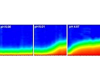
Washington DC (SPX) Jun 16, 2010 Using a chemical trick that allows them to change the acidity of a solution almost instantly, a team at the National Institute of Standards and Technology (NIST) has demonstrated a simple and effective technique for quantifying how the stability of nanoparticle solutions change when the acidity of their environment suddenly changes. The measurement method and the problem studied are part o ... read more |
|
| The content herein, unless otherwise known to be public domain, are Copyright 1995-2010 - SpaceDaily. AFP and UPI Wire Stories are copyright Agence France-Presse and United Press International. ESA Portal Reports are copyright European Space Agency. All NASA sourced material is public domain. Additional copyrights may apply in whole or part to other bona fide parties. Advertising does not imply endorsement,agreement or approval of any opinions, statements or information provided by SpaceDaily on any Web page published or hosted by SpaceDaily. Privacy Statement |


 del.icio.us
 Digg
Digg Reddit
 YahooMyWeb
 Google