|
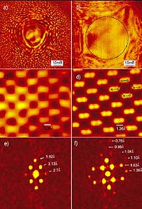
Yorktown Heights - August 8, 2002 IBM and Nion Co. researchers have developed innovative technology to peer deep inside materials and view atoms interacting in different environments at a resolution never before possible. With computer-chip features shrinking to atomic scales, this breakthrough addresses scientists' urgent need to see more clearly the details of materials used in manufacturing semiconductors. As reported in the August 8 issue of the journal Nature, the new technique significantly extends the capabilities of the electron microscope -- a scientific instrument that uses magnetic lenses to focus electrons into very small beams to look at small, atomic-scale details in thin slices of materials. "We can't fix what we can't see," said Dr. Philip Batson, the lead scientist on the project at IBM Research. "As the dimensions of computer chips shrink, scientists need new tools to explore the structures and properties of materials used in these chips. This breakthrough improves our ability to see and thoroughly explore properties of electronic materials." For the past 50 years, electron optics engineers have sought to improve the precision of electron microscopes by counteracting the image-blurring effects of lens imperfections, or "aberrations." The largest imperfection, "spherical aberration," cannot be fixed in a single lens. To fix the problem, the IBM and Nion scientists combined seven new sets of magnetic lenses with modern computers to actively correct the aberration in real-time. After this correction, the microscope can make an electron beam that is only 75 thousandths of a nanometer (3 billionths of an inch), which is smaller than a single hydrogen atom. This is the smallest electron beam produced in an electron microscope to date. Spying on Silicon for Smaller, Faster Computer Chips Before the correction, the electron microscope yielded tantalizing but incomplete information about the atomic structure of important defects -- atomic level mistakes such as missing or extra atoms -- in semiconductor materials. Using this correction technique, scientists now can see those defects, and if necessary, find ways to fix them. For example, by examining the interaction of silicon (a semiconductor) with silicon oxide (an insulator), scientists can look at how the silicon and oxygen atoms bond to each other and determine the quality of the insulator. If the insulator has any defects, scientists can suggest ways to fix them, such as setting the right conditions to optimize the growth of silicon and silicon oxide materials. The breakthrough could also help scientists improve the properties of silicon through a better understanding of how the atoms inside of materials interact in certain environmental conditions. Watching how atoms assemble, move around and interact with other atoms is fundamental to understanding the properties of materials and may lead to a better understanding of how to control environmental conditions so components of future computer chips could self-assemble. The authors of the Nature report, entitled "Sub-angstrom Resolution Using Aberration Corrected Electron Optics," are Philip E. Batson of IBM's T.J. Watson Research Laboratory in Yorktown Heights, N.Y; and Niklas Dellby and Ondrej L. Krivanek of Nion Co. in Kirkland, Washington. Community Email This Article Comment On This Article Related Links SpaceDaily Search SpaceDaily Subscribe To SpaceDaily Express Space Technology News - Applications and Research
 Baltimore MD (SPX) Jan 12, 2006
A team comprised of three leading US aerospace and defense contractors has demonstrated an innovative technological use of active electronically scanned array (AESA) radars for high-bandwidth communications. |
|
| The content herein, unless otherwise known to be public domain, are Copyright 1995-2006 - SpaceDaily.AFP and UPI Wire Stories are copyright Agence France-Presse and United Press International. ESA PortalReports are copyright European Space Agency. All NASA sourced material is public domain. Additionalcopyrights may apply in whole or part to other bona fide parties. Advertising does not imply endorsement,agreement or approval of any opinions, statements or information provided by SpaceDaily on any Web page published or hosted by SpaceDaily. Privacy Statement |