|
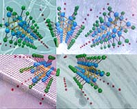
San Francisco - Feb 6, 2002 An entirely new generation of powerful ultra-small computers and electronic devices is one step closer, according to researchers at the University of California-Berkeley. Their work, and that of a Swedish team, is reported in the February issue of the peer-reviewed journal Nano Letters, published by the American Chemical Society, the world's largest scientific society. The two groups have succeeded independently in making lattices that they say will for the first time enable nanowires to be constructed with otherwise incompatible materials. Such mixed bundles are essential to making electronics and other devices on an increasingly smaller scale. "This is a major advancement in the field of one-dimensional nanostructure research. The impact could be tremendous," predicts Peidong Yang, Ph.D., assistant professor in the Department of Chemistry at the University of California and a faculty scientist in the Materials Science Division at the Lawrence Berkeley National Laboratory. A related paper by Swedish researchers also appears in the February issue of Nano Letters. Based on the findings of both research groups, tiny components known as nanowires that meld together a variety of materials could soon be routinely and cheaply built using little more than a special mixture of gases deposited on a foundation material. The report by the U.S. team of three researchers details how they successfully fabricated "superlattice" nanowire, so named because the nanowire's cylinder-shaped nanoscopic bundle interweaves substances with different compositions and properties. As a result, well-defined junctions and interfaces with potentially important functionalities were incorporated within individual nanowires. Those working in the field of nanotechnology have long sought such a means to bring together materials on the nanoscopic scale that otherwise would be structurally incompatible. Like conventional builders � who rely on a mix of concrete, wood, metals, plastics and paints to construct comfortable and energy-efficient homes and offices � nanoengineers, by mixing and matching a m�lange of elements, hope to create entirely new classes of nanoscale products or systems that would revolutionize everything from energy production to manufacturing and assembly. In the field of electronics and optics, mastery of these nanoscale "heterostructures" should lead to devices too small to see with the naked eye, but equal to or better than today's hand-size electronics. The team of nine Swedish scientists working in the Materials Chemistry and Solid State Physics Departments in Lund University's Nanometer Consortium used related but different methods than their California peers. In both cases, manufacture is relatively straightforward and results in stable nanowires that can operate at room temperature, Yang reports. "Without a way of putting different materials together with a junction of some kind, we wouldn't have all the devices we take for granted, like transistors and [compact disc] lasers," he says. But the California scientists have gone a step further: "We've successfully made nanoscale junctions within individual [nano]wires, putting different materials together, embedding junctions directly in the wires. The next step is to use the wires as submicroscopic components for various optoelectronic devices. These are definite first steps, but critical ones." Today's personal computers rely on a series of small junctions that connect components that have properties necessary for proper functioning. Given the laws of physics and real-world manufacturing demands, radically scaling down such functionality is difficult. The research findings in California and Sweden promise to make ultra-small-scale devices practical. The newly reported research also should help allay concerns of those who worry that "Moore's Law" might not hold, considering the physical limits inherent in current approaches to computer-chip design. The law, first postulated by Gordon Moore, a physical chemist and cofounder of Intel Corporation, proposed that computer processing power would likely double every year or so. "Growing" a nanowire can be done either with vapor deposition from a stockpile of specialty gases, or with a laser aimed at a target material to produce a specific vapor, or both. In either case, the gases are directed toward and then condense on a substrate material, like silicon. Because the technique is precisely controlled, the resultant nanowire can be customized according to function or composition. Thus, single nanowires can control current flow, emit light, process or store information or dissipate heat � but at extremely small scales. Nanowire production is both rapid and economical. In just one hour, millions of nanowires can be made at minimal expense. Community Email This Article Comment On This Article Related Links Yang Lab SpaceDaily Search SpaceDaily Subscribe To SpaceDaily Express Nano Technology News From SpaceMart.com Computer Chip Architecture, Technology and Manufacture
 New York (UPI) Mar 18, 2005
One of the single biggest applications of nanotechnology could be solving the global shortage of pure water, experts told UPI's Nano World. |
|
| The content herein, unless otherwise known to be public domain, are Copyright 1995-2006 - SpaceDaily.AFP and UPI Wire Stories are copyright Agence France-Presse and United Press International. ESA PortalReports are copyright European Space Agency. All NASA sourced material is public domain. Additionalcopyrights may apply in whole or part to other bona fide parties. Advertising does not imply endorsement,agreement or approval of any opinions, statements or information provided by SpaceDaily on any Web page published or hosted by SpaceDaily. Privacy Statement |