|
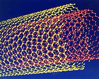
Rehovot, Israel (SPX) Jan 04, 2005 The Weizmann Institute of Science recently announced that a research group headed by Dr. Ernesto Joselevich has developed a new approach to create patterns of carbon nanotubes by formation along atomic steps on sapphire surfaces. Carbon nanotubes are excellent candidates for the production of nanoelectronic circuits, but their assembly into ordered arrays remains a major obstacle toward this application. The team was initially researching in a different direction: they were trying to give carbon nanotubes (structures reminiscent of rolled-up sheets of graphite) a preferred orientation on a wafer by applying an electrical field as the tubes were being formed. This works very well with silicon dioxide wafers. On a sapphire support (sapphire is a form of aluminum oxide), on the other hand, it didn't work: the nanotubes were beautifully arranged in parallel, but with an orientation that was completely independent of the electrical field � even when no field was applied at all. Closer examination of the sapphire surface solved the mystery: commercial sapphire wafers are generally not cut exactly along the plane of the crystal. Their surface is thus not completely smooth; instead, it has parallel steps � of atomic dimensions � between the different planes of the crystal. The nanotubes wind up lying along these steps. The researchers explain it like this: the nanotubes form from a catalyst of iron nanoparticles and are attracted to a local field created by the steps. It is clear that these iron particles don't like "climbing stairs;" instead, they "glide" along the inner edge of the step, as though on a track. Thus they remain continuously in contact with two surfaces, rather than just one, which seems to stabilize the catalyst. Just as an airplane leaves behind a condensation trail, the iron particles leave the newly formed nanotubes lying along their "tracks." The nanotubes even follow kinks in the steps, which are caused by defects in the crystal. This results in either straight or zigzag-shaped tubes, which are expected to have particularly interesting electronic properties. "The orientation and form of the atomic steps on a crystal surface can be controlled by the cutting process, and defects can be created artificially," says Joselevich. "It should thus be possible to produce different nanowire arrangements in a controlled fashion." Community Email This Article Comment On This Article Related Links Weizmann Institute SpaceDaily Search SpaceDaily Subscribe To SpaceDaily Express Nano Technology News From SpaceMart.com Computer Chip Architecture, Technology and Manufacture
 Evanston IL (SPX) Sep 23, 2005
The design, development and manufacturing of revolutionary products such as the automobile, airplane and computer owe a great deal of their success to the large-scale material testing systems (MTS) that have provided engineers and designers with a fundamental understanding of the mechanical behavior of various materials and structures. |
|
| The content herein, unless otherwise known to be public domain, are Copyright 1995-2006 - SpaceDaily.AFP and UPI Wire Stories are copyright Agence France-Presse and United Press International. ESA PortalReports are copyright European Space Agency. All NASA sourced material is public domain. Additionalcopyrights may apply in whole or part to other bona fide parties. Advertising does not imply endorsement,agreement or approval of any opinions, statements or information provided by SpaceDaily on any Web page published or hosted by SpaceDaily. Privacy Statement |