|
New York (UPI) June 30, 2005 A new method to carve infinitesimal gaps into nanowires soon could help scientists connect electronics to single molecules. This in turn could lead to computers based on molecular transistors with vastly greater computing power than conventional machines. Researchers at Northwestern University in Chicago who are developing the technique already have created notches only 2.5 nanometers wide - or 2.5 billionths of a meter, the breadth of a DNA molecule - in gold nanowires, into which a variety of compounds, such as genes, could be plugged. "I believe we'll hit 1 nanometer within the year," senior researcher Chad Mirkin told UPI's Nano World. Researchers want to connect electronics with single molecules for a number of reasons. For instance, if they wire up molecules that recognize specific genes or viruses, they could create devices that sequence genomes electronically or detect bioweapons. Electronics giants such as Hewlett-Packard, Motorola and IBM are conducting research and development into molecular electronics, where individual molecules serve as elements of circuits. "These molecules are several times smaller than the best structures you can make in silicon today," Charles Martin, director of the Center for Research at the Bio/Nano Interface at the University of Florida in Gainesville, told Nano World. "This means you could pack many, many more circuit elements per square centimeter of chip surface," leading to more powerful computers. One major challenge is how to accomplish the electronics-molecular connection. The standard procedure is to create gaps in nanowires, into which molecules are plugged, but prior techniques have required sophisticated, expensive microfabrication, experimental finesse, and often have yielded only a small number of functional devices. Mirkin and his team have invented a process they call on-wire lithography, or OWL. It involves creating nanowires from long segments of gold connected by short bits of silver or nickel. The nanowires are then bound to layers of silicon dioxide on a foundation layer. The nickel or silver is etched off with nitric acid, leaving the gold nanowire and gaps. The researchers very carefully vary the length of each segment, with the length of the dissolved nickel equaling the length of the desired gap in the gold nanowire. Mirkin and colleagues described the process in the July 1 issue of the journal Science. "This approach is fast, very controllable, high yielding and low cost," Mirkin said. "People in this field struggle with conventional lithographic tools to make structures analogous to some of the ones we can make routinely with OWL. The method is not only powerful from a technological standpoint, but also almost accessible to anyone with some experience in chemistry and very low-cost equipment, as opposed to a billion-dollar fab line." The team plugs each gap in the nanowire using a method they invented called dip-pen lithography, which draws nanometer-sized features using pen tips dipped into wells of ink made of virtually any material desired. "This is a fantastic idea that is so simple, so elegant," Martin, who did not participate in the research, told Nano World. "Controlling matter at this length scale opens lots and lots of doors." Mirkin noted his team is considering whether to begin a new startup company based on their method or license the technology to larger companies. They will decide after conducting more experimentation. Charles Choi covers research and technology for UPI Science News. E-mail: [email protected] Community Email This Article Comment On This Article Related Links SpaceDaily Search SpaceDaily Subscribe To SpaceDaily Express Nano Technology News From SpaceMart.com Computer Chip Architecture, Technology and Manufacture
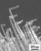 San Diego CA (SPX) Apr 12, 2005
Researchers at UCSD have made carbon nanotubes bent in sharp predetermined angles, a technical advance that could lead to use of the long, thin cylinders of carbon as tiny springs, tips for atomic force microscopes, smaller electrical connectors in integrated circuits, and in many other nanotechnology applications. |
|
| The content herein, unless otherwise known to be public domain, are Copyright 1995-2006 - SpaceDaily.AFP and UPI Wire Stories are copyright Agence France-Presse and United Press International. ESA PortalReports are copyright European Space Agency. All NASA sourced material is public domain. Additionalcopyrights may apply in whole or part to other bona fide parties. Advertising does not imply endorsement,agreement or approval of any opinions, statements or information provided by SpaceDaily on any Web page published or hosted by SpaceDaily. Privacy Statement |