|
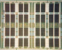
New York (UPI) Jan 31, 2005 In the next decade, the leading method of data storage could be nanotechnology-based magnetic RAM or MRAM, which is expected to grow to a market of $2.1 billion by 2008 and $16.1 billion by 2012. The most surprising thing to me is how soon this looks like it's coming, and how many companies there actually are looking at it as a commercial prospect, Lawrence Gasman, principal analyst for NanoMarkets, an industry research firm in Sterling, Va., told UPI's Nano World. It will probably be overhyped like these kinds of things always are, but it looks like a nice little sector is emerging here. Unlike all other existing computer memories, which are based on storing electrical charge, MRAM stores information using magnetic bits, each akin to a compass needle. A computer writes data into MRAM by flipping each bit's magnetic polarity. Because these bits are tiny permanent magnets, this information remains when the electrical power is removed from the chip, explained Saied Tehrani, director of MRAM technology at Freescale in Austin, Texas, the semiconductor products sector of Motorola. On the other hand, dynamic and static RAM - also known as DRAM and SRAM, the most common types of memory in use today - are volatile and require a continuous supply of electricity. Flash memory, which is most familiar to digital camera enthusiasts, is non-volatile like MRAM. Flash stores information by trapping charge that has been transported across a physical barrier. This transporting of charge requires higher voltages and has a known limited lifetime due to wear-out of the barrier after as little as 100,000 write cycles, Tehrani told Nano World. The magnets in MRAM, on the other hand, can be switched indefinitely with no known wear-out. Also, because MRAM can be directly programmed in a few nanoseconds, it is extremely fast compared with Flash, which takes milliseconds to program and also requires a separate erase cycle, Tehrani said. In addition, while it can be as fast as SRAM, MRAM can in theory achieve higher density, since MRAM only has one transistor per cell while SRAM uses six to achieve its high speed. Moreover, unlike electrically based memory, MRAM is not sensitive to erasure from radiation, making it valuable for military and satellite applications. MRAM is a technology that uniquely combines the best attributes of other current memory technologies into one, low-cost solution, Tehrani said. Nearly 20 firms are active with MRAM, with 2005 the first year we'll see some real revenues with MRAM, Gasman said, with Cypress Semiconductor in San Jose, Calif., expecting $2 million from the technology this year. IBM, Infineon, Freescale and Cypress also are pursuing early entry with MRAM products, while NEC, Toshiba, Samsung, Sony and Taiwan Semiconductor are looking at later entries and Honeywell is pursuing specialist applications. Also, Hewlett-Packard looks to license MRAM intellectual property, while Philips is supplying non-MRAM technology to MRAM suppliers. In 2006, Gasman expects demand for MRAM to grow. Such chips could help notebook computers, PDAs and cell phones rapidly power up to the exact point they were when they were turned off. MRAM also could help microcontrollers and robots in factory automation, replacing both RAM and PROMs/Flash, and find its way into radio-frequency identification tags via Micromem in Toronto. RFID tags allow companies to track inventory more quickly and precisely, helping to save an industry giant such as Wal-Mart $1.3 billion to $1.5 billion annually, according to AMR Research in Boston. Difficulties remain on the road to MRAM, however. The first generation of MRAM chip, at 4 megabits or 8 megabits, is well below a current 1-gigabit Flash chip. It's a very long way behind conventional RAM technologies, Gasman said. Improving that doesn't happen overnight, and it has a moving target to catch up with - Flash is getting better. This problem of scaling up MRAM is one of the reasons Intel is not pursuing the technology. The materials used for the magnetic memory effect themselves have certain scaling issues, Intel memory technology development group member Greg Atwood told Nano World. Also, the power required to generate a magnetic field to write onto MRAM requires a pretty high current, perhaps milliamps, which is a very high current for such small devices. And the current you need doesn't scale down as the size goes down. Gasman disagreed. Toshiba, IBM and NEC would not put a lot of money into this space without the belief they can upgrade the technology, he said, and Intel's never really made a commitment to MRAM. Still, Gasman noted Micron Technology in Boise, Idaho, did invest in MRAM only to withdraw, instead pursuing a nanocrystalline version of Flash technology. He also noted that MRAM remains expensive. As far as I can determine, there's nothing intrinsically expensive about it, though, he said. This should change as the volume production ramps up. The other issue you hear is that you need to create very fine magnetic layers, and if you build them too thin you get lots of errors due to interference effects, and if you build them too thick it doesn't work. So it's a yield issue, but it's the kind of thing that changes with experience. Gasman said in the long-term, MRAM companies might also face legal challenges. NVE in Eden Prairie, Minn., which sells nanosensors and related devices, licensed its MRAM technology to three companies: Agilent, Motorola and Cypress. The interesting thing is Motorola-Freescale, he said. NVE is now trying to renegotiate so their agreement applies with Freescale, a legal challenge in the making, and some figures with investment interest, such as banks, have made the point that Motorola has partnerships in MRAM, such as with Philips and Taiwan Semiconductor, and these partners might have to pay money to NVE. So that's completely unclear. The issue could end up in court, Gasman said. The type of thing that drags on for a couple of years. The impact of that is not attractive. Still, most companies, such as IBM and Toshiba, have no connections with NVE, and will not be drawn into any lawsuit.
Community
 Pittsburgh PA (SPX) Jun 23, 2005
When light hits a semiconductor material and is absorbed, its photons can become "excitons," sometimes referred to as "heavy photons" because they carry energy, like photons, but have mass, like electrons. |
|
| The content herein, unless otherwise known to be public domain, are Copyright 1995-2006 - SpaceDaily.AFP and UPI Wire Stories are copyright Agence France-Presse and United Press International. ESA PortalReports are copyright European Space Agency. All NASA sourced material is public domain. Additionalcopyrights may apply in whole or part to other bona fide parties. Advertising does not imply endorsement,agreement or approval of any opinions, statements or information provided by SpaceDaily on any Web page published or hosted by SpaceDaily. Privacy Statement |