|
New York (UPI) Aug 10, 2005 Semiconductor industry tools and instruments that work on the nanoscale could form a $5.5 billion market by 2012, experts told UPI's Nano World. "Without the growing toolbox of techniques that enable things to be created at the nanoscale, nanotechnology doesn't exist, and a lot of these tools are coming from the semiconductor industry," said Lawrence Gasman, principal analyst for NanoMarkets, an industry research firm in Sterling, Va. To keep computer power steadily advancing, as it has been for the last 30 years, the electronics industry is shrinking microchip features to 90 nanometers. Based on Moore's Law - the industry's observed capability to double transistor density roughly every two years - the 10-nanometer limit should arrive in roughly 15 years. The practical limit on feature size for optical projection lithography, the technique currently used to manufacture high-performance chips, is roughly 65 nanometers. Given Moore's Law, this platform should prove obsolete by 2007. To meet this challenge, "there are now a growing number of alternatives to conventional lithography that are being developed for making silicon microelectronics," Gasman said. "All of them have considerable promise, but they will be expensive to develop and fully commercialize. In many cases, they are more suitable for R&D than volume production." Extreme ultraviolet lithography employs ultraviolet lasers, and can in theory operate down to 13 nanometers, but has experienced "numerous teething problems which seem to have put off most backers except Intel," Gasman said. Electron projection lithography uses electron sprays that are difficult to focus, said Will Arora, senior associate at Lux Research in New York City. "The biggest retarding factor is lack of customer interest at the present time," Gasman said. Optical projection lithography works by shining a laser through lenses and a pattern of transistor features onto a light-sensitive "photoresist" layer atop a silicon wafer. A similar technology, known as immersion lithography, works by placing a layer of water between the last lens and the silicon, which bends the light and leads to sharper features. Lithography market leaders ASML, Canon and Nikon have announced plans to ship commercial immersion lithography tools by 2006, Lux Research reported. "It may be very useful at 32 nanometers, but have weak legs beyond that," Gasman said. "Immersion lithography is simpler, faster and potentially far more cost efficient than completely retooling your (fabricator) using extreme ultraviolet," said Nathan Tinker, co-founder and executive vice president of the NanoBusiness Alliance in New York. Semiconductor lithography equipment should lead to a nearly $3.8 billion market by 2012, but semiconductor nanotech equipment probably will create a $1.7 billion sector with technologies that write features directly onto chips, Gasman said. For instance, nanoimprint lithography directly presses a hard mask onto a photoresist to stamp the pattern physically without using expensive and cumbersome optics or lasers. The method can create perfect patterns down to 10 nanometers with "excellent economics," he noted. In 2002 Motorola became the first large semiconductor manufacturer to test a nanoimprint tool, and key infrastructure companies such as KLA Tencor and LAM Research - which are vital to supporting any new lithography technique - have begun signing partnerships with nanoimprint vendors such as EVG, Molecular Imprints, Nanonex, Obducat and SUSS MicroTec, Arora said. Another potentially revolutionary technology is dip-pen lithography, which draws features nanometers in size using infinitesimal pen tips dipped into wells of ink made of virtually any desired chemical. The technique has "a broad range of applications both within semiconductors and electronics and in the life sciences," Gasman said. "If they can get it scaled up, it could steamroll everything else out there," Tinker added. Part 1 of 2. Community Email This Article Comment On This Article Related Links SpaceDaily Search SpaceDaily Subscribe To SpaceDaily Express Nano Technology News From SpaceMart.com Computer Chip Architecture, Technology and Manufacture
 Newark DE (SPX) Oct 14, 2005
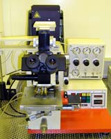
University of Delaware researchers are opening a new front in the war on cancer, bringing to bear new nanotechnologies for cancer detection and treatment and introducing a unique nanobomb that can literally blow up breast cancer tumors. |
|
| The content herein, unless otherwise known to be public domain, are Copyright 1995-2006 - SpaceDaily.AFP and UPI Wire Stories are copyright Agence France-Presse and United Press International. ESA PortalReports are copyright European Space Agency. All NASA sourced material is public domain. Additionalcopyrights may apply in whole or part to other bona fide parties. Advertising does not imply endorsement,agreement or approval of any opinions, statements or information provided by SpaceDaily on any Web page published or hosted by SpaceDaily. Privacy Statement |