|
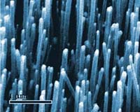
Moffett Field - Apr 15, 2003 The life of the silicon chip industry may last 10 or more years longer, thanks to a new manufacturing process developed by NASA scientists. The novel method, announced in the April 14 issue of the journal Applied Physics Letters, includes use of extremely tiny carbon 'nanotubes' instead of copper conductors to interconnect parts within integrated circuits (ICs). Carbon nanotubes are measured in nanometers, much smaller than today's components. A nanometer is roughly 10,000 times smaller than the width of an average human hair. ICs are very small groups of electronic components made on silicon wafers. "NASA needs high-performance computing in small packages for future autonomous spacecraft," said Meyya Meyyappan, director of the Center for Nanotechnology at NASA's Ames Research Center (ARC), Moffett Field, Calif., coauthor of the article. "The bottom line is that computer chips with more layers and smaller components can do more for us. While we are working on carbon nanotube-based chips for long-term needs, we also are indirectly helping industry to keep silicon-based computer chips in use as long as possible," he said. One advantage of using carbon nanotube interconnects within integrated circuits is that these interconnects have the ability to conduct very high currents, more than a million amperes of current in a one square centimeter area without any deterioration, which seems to be a problem with today's copper interconnects," said Jun Li, lead scientist of the team at ARC that developed the new process. "Also, there is no need to create deep, narrow trenches on silicon wafers in which to bury copper conductors, a step that also is becoming a problem as components are made smaller and smaller," Li added. "Our process allows us to use the tiny carbon nanotubes to replace copper to interconnect network layers on silicon chips," Meyyappan said. "We think this new process may well help to sustain the Moore's Law growth curve." Moore's Law stemmed from an observation made by computer chip pioneer Gordon Moore in 1964 that the number of transistors in a given area of an IC had doubled every year since its invention. Moore predicted the trend would continue at a rate of about 18 months between doublings. Continuing down this 'doubling' path is becoming increasingly difficult, according to Meyyappan. "Roadblocks exist in several common technologies such as interconnects, lithography and others currently used to make the chips," he said. "However, I think our new process could be in use by industry for the next generation of ICs, removing some of these roadblocks," Meyyappan added. "Using the new process, manufacturers will be able to add more cake-like layers of components to silicon chips to increase computer capability," Li said. Because copper's resistance to electricity flow increases greatly as the metal's dimensions decrease, there is a limit to how small copper conductors can be. In contrast, extremely tiny carbon nanotubes can substitute for copper conductors in smaller computer chip electronic configurations, because carbon nanotube electrical resistance is not high. The new process includes 'growing' microscopic, whisker-like carbon nanotubes on the surface of a silicon wafer by means of a chemical process. Researchers deposit a layer of silica over the nanotubes grown on the chip to fill the spaces between the tubes. Then the surface is polished flat. Scientists can build more multiple, cake-like layers with vertical carbon nanotube 'wires' that can interconnect layers of electronics that make up the chip. Community Email This Article Comment On This Article Related Links Nanotechnology at NASA SpaceDaily Search SpaceDaily Subscribe To SpaceDaily Express Space Technology News - Applications and Research
 Baltimore MD (SPX) Jan 12, 2006
A team comprised of three leading US aerospace and defense contractors has demonstrated an innovative technological use of active electronically scanned array (AESA) radars for high-bandwidth communications. |
|
| The content herein, unless otherwise known to be public domain, are Copyright 1995-2006 - SpaceDaily.AFP and UPI Wire Stories are copyright Agence France-Presse and United Press International. ESA PortalReports are copyright European Space Agency. All NASA sourced material is public domain. Additionalcopyrights may apply in whole or part to other bona fide parties. Advertising does not imply endorsement,agreement or approval of any opinions, statements or information provided by SpaceDaily on any Web page published or hosted by SpaceDaily. Privacy Statement |