|
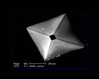
Murray Hill - Aug. 30, 2001 Electronic components, such as transistors on computer chips, are increasingly becoming smaller, while their performance capabilities are growing. It is expected that the dimensions of such components will be in the nanometre range from as early as 2010. However, once the dimensions are in the realm of nanometres, the semiconductor properties are subject to the laws of quantum mechanics and are, for instance, dependent on the geometric dimensions of the components. At the Institute for Semiconductor and Solid State Physics at the University of Linz, G�nther Bauer's team has, with the support of the Austrian Science Fund, succeeded in producing and characterising such semiconductor nanostructures. The Linz physicists envisage that one of the first areas of application will be in laser technology. A nanometre is roughly equivalent to one hundred-thousandth of the diameter of a human hair. In as little as approximately ten years' time, the electronic industry will be using semiconductor components which measure approximately 30 to 50 nanometres and which possess the necessary properties for the relevant application. The Linz team can produce such miniature structures in a controlled process and determine their properties. "There are two production methods: with the 'top down' method, different semiconductor materials such as silicon and germanium are grown on top of one another, thus forming a type of sandwich structure which is subsequently processed by means of lithography and etching. "The electrical, optical and magnetic properties of these structures depend not only on the chemical composition, but also on the thickness and distortion of the layers," explains Bauer. "With the 'bottom up' method, small, pyramid-shaped islands, measuring approximately 10 nanometres in height, are produced through so-called self-organised growth." Since a temperature of approximately 600 degrees is required for the precipitation of these islands, the starting materials are automatically mixed and the germanium concentration increases from the base of the pyramid towards the tip. However the ratio of ingredients in turn influences the quantum mechanical properties, so the control of this ratio is therefore important.
Tomography for nano-pyramids Thanks to this success, the possibility of an application for the middle infrared, e.g. in laser technology, becomes feasible. "The pyramids could be installed in resonators to create lasers which work with lower threshold currents than conventional lasers. This would certainly extend the service life of such components considerably," says Bauer. Further research into the controlled growth and the structural, electronic and optical properties of such nano-components is certainly required over the coming years. Community Email This Article Comment On This Article Related Links Institute for Semiconductor and Solid State Physics - Linz SpaceDaily Search SpaceDaily Subscribe To SpaceDaily Express Carbon Worlds - where graphite, diamond, amorphous, fullerenes meet
 Taunton MA (SPX) Jan 5, 2006
Kopin and ExPlay have announced that they are in development of an ultra-small nano projector based on an ultra-high-efficiency version of Kopin's microdisplay, which is being specifically designed for the nano projector, and ExPlay's unique optical technology. |
|
|
|
|
|
|
|
|
|
|
|
|
|
| The content herein, unless otherwise known to be public domain, are Copyright 1995-2006 - SpaceDaily.AFP and UPI Wire Stories are copyright Agence France-Presse and United Press International. ESA PortalReports are copyright European Space Agency. All NASA sourced material is public domain. Additionalcopyrights may apply in whole or part to other bona fide parties. Advertising does not imply endorsement,agreement or approval of any opinions, statements or information provided by SpaceDaily on any Web page published or hosted by SpaceDaily. Privacy Statement |