|
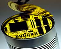
Belgium (SPX) Aug 19, 2005 A recent EU project designed and developed a new demonstrator microchip that will dramatically cut the cost of producing new wireless products and could mean that a whole range of existing products will be enabled for wireless communication. The IST-funded IMPACT project included industry heavyweights Ericsson and Philips who worked together to develop a new CMOS (complementary metal-oxide-semiconductor) chip that can transmit and receive microwave signals in the 5�24 GHz frequency range. The team developed a range of demonstrators, including amplifiers, oscillators, mixers, and frequency multipliers. The IMPACT team sought to discover whether analogue and radio frequency (RF) circuits could be developed for the emerging 90nm CMOS chips. These chips use a much smaller (90nm) circuit etching process than current models. "The 90 nm digital CMOS chips are becoming available this year and we wanted to know if we could use them for high-frequency microwave communications," says Dr Stefaan Decoutere, coordinator of the IMPACT project and a researcher at the Interuniversity MicroElectronics Centre (IMEC) in Belgium. Older RF-CMOS chips are already used in 2.4Ghz devices like the Bluetooth transmitters and receivers developed separately by Ericsson, one of the project partners. "But the requirements for high-end applications like GSM telephony are much more stringent," says Decoutere. Currently these applications require expensive, multi-chip solutions. IMPACT found that the 90nm CMOS chips can meet the stringent specification standards for mid-range and high-end applications like GSM and Point-to-Point microwave communications. Ultimately it will cut costs, reduce power consumption and increase the functionality of these devices. "These chips are expensive to develop but over time they are much cheaper to produce," says Decoutere. Because all the circuits are on one chip the production process is much more efficient and RF-CMOS chips can be produced in large volumes, slashing costs.
High potential The potential for CMOS chips in microwave communications is excellent, according to Professor Herbert Zirath, an IMPACT member at Chalmers University of Technology in Sweden. "CMOS can be used for radio communication and radar circuits like mobile phones, wireless local area networks (WLAN), high speed links, where many functions are integrated. This will be important for the cost of such systems since CMOS is very cost efficient in large quantities." CMOS chips are an important type of integrated circuits. They include microprocessors, microcontrollers, static RAM, and other digital circuits. These different functions can be integrated on a single chip, further reducing costs and the complexity of devices like digital cameras. CMOS chips only use power when its transistors are switching between on and off states. As a result, they use less electricity and generate less heat than rival chips, which means they are ideal for mobile applications.
Pushing state-of-the-art The IMPACT team scored two successes. Firstly, they achieved a given performance specification at significantly lower cost and power consumption than can be managed with today's technologies. Secondly, they pushed the state-of-the-art circuit performance in RF-CMOS technology with demonstrator low-noise amplifiers and voltage-controlled oscillators with world-record figures-of-merit in performance and robustness against Electrostatic Discharge. The project won the enthusiastic support of the industrial partners. Ericsson said the project fell well within its strategic vision for the exploitation of the microwave frequency spectrum and that a major advantage was that project began with specific applications in mind. "The review for the European Commission was very positive and we produced nearly 50 papers on our research in international conferences and journals," says Decoutere. The project may even be chosen for the EC 2005 research yearbook, which highlights outstanding research in the EU. Applications for the 90nm CMOS technology are already in the works. For example, Ericsson's target applications over the next three years include WLAN systems, like WiFi, and terminals in the 5 to 6 GHz frequency range. Project partner Philips says that the use of mainstream CMOS technology as a cost-effective solution for wireless communication is a particularly important emerging market with a huge range of potential product applications. Philips believes this technology will become an enabler for wireless consumer electronics and that virtually all-electronic products may become wireless so as to enable device-to-device interaction. This not only includes high-end and luxury products, as are available now, but also but also low-end products such as Walkmans and MP3 players. But these devices are heavily dependent on the timely integration of RF and analogue functionality into advanced CMOS technology in order to yield cost-effective system-on-a-chip solutions. IMPACT has gone a long way to solving these problems. In the meantime, IMPACT wants to launch a follow-up project to see if it is possible to develop CMOS chips using a 45nm etching process. "If you look at scaling of digital CMOS you see that scaling towards 65 nm follows more or less the same approaches used in earlier chips," says Decoutere. "But for 45 nm and below there are quite a number of new materials and new architectures that are under investigation. We want to see what effect the new materials and production technologies required to produce a 45 nm chip might have on analogue and radio frequency functionality." Advantages in a 45nm CMOS chip could include smaller chip size, the potential for improved performance, and lower power consumption for the same functionality, if the researchers can get it to work. Community Email This Article Comment On This Article Related Links SpaceDaily Search SpaceDaily Subscribe To SpaceDaily Express Computer Chip Architecture, Technology and Manufacture Nano Technology News From SpaceMart.com
 West Lafayette IN (SPX) Aug 17, 2005
Engineers at Purdue University have created a nanotech simulation tool that shows how current flows between silicon atoms and individual molecules to help researchers design "molecular electronic" devices for future computers and advanced sensors. |
|
| The content herein, unless otherwise known to be public domain, are Copyright 1995-2006 - SpaceDaily.AFP and UPI Wire Stories are copyright Agence France-Presse and United Press International. ESA PortalReports are copyright European Space Agency. All NASA sourced material is public domain. Additionalcopyrights may apply in whole or part to other bona fide parties. Advertising does not imply endorsement,agreement or approval of any opinions, statements or information provided by SpaceDaily on any Web page published or hosted by SpaceDaily. Privacy Statement |