|
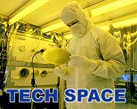
Troy - Sep 01, 2003 Researchers led by Ronald J. Gutmann in the Focus Center-New York at Rensselaer (FC-NY-RPI) are pioneering new interconnect technologies that promise to deliver smaller, faster, inexpensive, microelectronics and circuits that function in three dimensions. Researchers at Rensselaer�s Focus Center-NY for Interconnections for Gigascale Integration believe that a strategy in which several chip wafers are bonded together in 3-D and interconnected provides an effective means to integrate chip technologies, and will dramatically improve performance and function. Working with collaborators from the semiconductor industry and other universities, the Rensselaer team is developing more effective interconnects that will allow information to get where it�s going more quickly and make computing ever faster. Jian-Qiang "James" Lu, a research associate professor of physics and electrical engineering, presented some of their findings in a paper co-authored with International SEMATECH (Austin, Texas) at the International Interconnect Technology Conference (IITC) in June. "At Rensselaer, we�re working with others to develop a very promising approach to building vertically integrated (3D) circuits; going up instead of across", says Lu. Vertical Bridges to the Next Level An interconnect is essentially a vertical bridge to another level. But it�s nearly impossible to keep building such bridges in two dimensions, Lu explains, because bridges span a chip similar to the way the Brooklyn Bridge spans the East River. "It�s a matter of necessity to consolidate space on a chip. Since real estate is dwindling as chip size decreases, the only way to go it seems, is up," says Lu. "If you�re in a city, like New York for example, and you want to increase and expand the scale of your business, you need to increase real estate, narrow the streets, and build bridges. But New York City is only so big, so you need to build skyscrapers. It�s the same with chips, Rensselaer is attempting to build the information bridges for the chip skyscrapers." If you want the signal to travel from one side of the chip to the other, there will be a delay because the global circuit wire is so long in 2-D (typically travel is 10,000 microns). One simple solution to interconnectivity is to cut that large chip to several small chips, then stack and connect them vertically. By cutting and stacking interconnects you can slash that global travel distance to 10 microns or less (chip-to-chip). Damascene Processing To make and interconnect 3-D chips, Lu explains Rensselaer�s process of effectively bonding wafers together face-to-face. After bonding and thinning the top wafer, inter-wafer interconnects are formed using the industry standard "damascene" processing. This process includes drilling a hole using dry etching, filling it with copper (the industry standard material), and polishing away extra copper define the metal lines that will carry signals around the "stacked-chip" product. Gutmann was a leader in developing this damascene process for defining metal lines. This damascene interconnect formation process, combined with wafer alignment, bonding and thinning, can be repeated for the third wafer, says Lu. "We're developing monolithic wafer-level 3-D integration processes that potentially can achieve all the advantages of system-on-a-chip and system-in-a-package, while lowering cost, enabling the use of small form factors and achieving high performance," Lu said. Hyper-Integration Further advancements and benefits of such a system on a 3-D chip are that each layer can be optimized for any given technology, meaning in one 3-D chip you could integrate (hyper-integrate) terahertz technology, mixed signal processing, wireless and optical systems. "Mixing the systems on a 3-D chip will enable technology for future chips to be low-cost and will also allow nanoelectronic, opto-electronic, and biochemical circuits to be integrated into heterogeneous systems," says Lu. Several RPI faculty members lead design, modeling and applications-oriented efforts that support different aspects of this fairly large effort. Also, the development cycles of various technologies using 3-D technology can be combined which compresses manufacturing time. Currently the cycles are dependant upon each other on a 2-D chip. With 3-D technology you can pick off-the-shelf technologies and plug them in, manipulating each layer separately and optimizing it to the needs of the user, explains Lu. Community Email This Article Comment On This Article Related Links Rensselaer Polytechnic Institute Process Evolution SpaceDaily Search SpaceDaily Subscribe To SpaceDaily Express Space Technology News - Applications and Research
 Baltimore MD (SPX) Jan 12, 2006
A team comprised of three leading US aerospace and defense contractors has demonstrated an innovative technological use of active electronically scanned array (AESA) radars for high-bandwidth communications. |
|
| The content herein, unless otherwise known to be public domain, are Copyright 1995-2006 - SpaceDaily.AFP and UPI Wire Stories are copyright Agence France-Presse and United Press International. ESA PortalReports are copyright European Space Agency. All NASA sourced material is public domain. Additionalcopyrights may apply in whole or part to other bona fide parties. Advertising does not imply endorsement,agreement or approval of any opinions, statements or information provided by SpaceDaily on any Web page published or hosted by SpaceDaily. Privacy Statement |