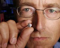
University of California Santa Barbara Professor John Bowers holds a Hybrid Silicon Laser chip
University of California Santa Barbara Professor John Bowers holds a Hybrid Silicon Laser chip |
"This breakthrough addresses one of the last major barriers to producing low-cost, high-bandwidth silicon photonics devices for use inside and around future computers and data centers," the company said in a statement.
The use of photonics, or optical data transfer, could vastly increase the speed of computers while keeping costs down, the researchers said.
Experts say the use of lasers could allow communication between chips within a system, bypassing many of the bottlenecks on existing computer chips.
"This could bring low-cost, terabit-level optical 'data pipes' inside future computers and help make possible a new era of high-performance computing applications," said Mario Paniccia, director of Intel's Photonics Technology Lab.
"While still far from becoming a commercial product, we believe dozens, maybe even hundreds of hybrid silicon lasers could be integrated with other silicon photonic components onto a single silicon chip."
The researchers said the key to manufacturing the device is the use of a low-temperature oxygen plasma -- an electrically charged oxygen gas -- to create a thin oxide layer on the surfaces of the materials.
Community
| The content herein, unless otherwise known to be public domain, are Copyright 1995-2006 - SpaceDaily.AFP and UPI Wire Stories are copyright Agence France-Presse and United Press International. ESA PortalReports are copyright European Space Agency. All NASA sourced material is public domain. Additionalcopyrights may apply in whole or part to other bona fide parties. Advertising does not imply endorsement,agreement or approval of any opinions, statements or information provided by SpaceDaily on any Web page published or hosted by SpaceDaily. Privacy Statement |