 |
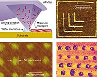
Evanston IL (SPX) Apr 27, 2005 The first practical fountain pen was invented in 1884 by Lewis Waterman. Although pens with self-contained ink reservoirs had existed for more than a hundred years before his invention, they suffered from ink leaks and other troubles. Waterman solved these problems by inventing the capillary feed which produced even ink flow. Now fountain pen history is repeating itself in the tiny world of nanoscale writing. Researchers at Northwestern University have demonstrated writing at the sub-100 nanometer molecular scale in fountain-pen fashion. They developed a novel atomic force microscope (AFM) probe chip with an integrated microfluidic system for capillary feeding of molecular ink. Their results are published online by Small, a new journal dedicated to breakthroughs in nanoscience and engineering. Dip-pen nanolithography (DPN) has been well-known for its capability of high-resolution direct writing as a bottom-up nanofabrication technique. The DPN technique exploits controlled deposition of molecules from an AFM tip to a surface. However, the need of replenishing ink whenever exhausted has been a limiting feature. Various attempts have been reported to overcome such a drawback, but none of them reached molecular patterns with features smaller than 100 nanometers. The Nanofountain Probe (NFP) developed by Horacio D. Espinosa, professor of mechanical engineering, and his colleagues employs a volcano-like dispensing tip and capillary fed solutions to enable sub-100 nanometer molecular writing. The NFP was microfabricated on a chip to be mounted on commercially available AFMs. The device consists of an on-chip reservoir, microchannels and a volcano-like dispensing tip. The microchannels are embedded in the AFM cantilevers of the chip and the volcano dispensing tip has an annular aperture to guide ink dispensing. The ink on the reservoir is driven through the microchannel via capillary action to reach the dispensing tip. At present, the smallest feature width achieved with the device is 40 nanometers. The standard microfabrication techniques used for the NFP chip - an important feature of this development - provides scalability to massively parallel arrays of probes and reservoirs for high throughput patterning with multiple molecular inks. "The writing capability of such NFP arrays with chemical and bimolecular inks in fountain-pen mode is unique," said Espinosa. "We believe the technology will likely lead to many high-impact applications in the field of nanosensors, biotechnology and pharmaceuticals." In addition to Espinosa, other authors on the Small paper are graduate student Keun-Ho Kim and research assistant professor of mechanical engineering Nicolaie A. Moldovan, both from Northwestern. Community Email This Article Comment On This Article Related Links Northwestern University SpaceDaily Search SpaceDaily Subscribe To SpaceDaily Express Nano Technology News From SpaceMart.com Computer Chip Architecture, Technology and Manufacture
 Newark DE (SPX) Oct 14, 2005
University of Delaware researchers are opening a new front in the war on cancer, bringing to bear new nanotechnologies for cancer detection and treatment and introducing a unique nanobomb that can literally blow up breast cancer tumors. |
|
| The content herein, unless otherwise known to be public domain, are Copyright 1995-2006 - SpaceDaily.AFP and UPI Wire Stories are copyright Agence France-Presse and United Press International. ESA PortalReports are copyright European Space Agency. All NASA sourced material is public domain. Additionalcopyrights may apply in whole or part to other bona fide parties. Advertising does not imply endorsement,agreement or approval of any opinions, statements or information provided by SpaceDaily on any Web page published or hosted by SpaceDaily. Privacy Statement |
