|
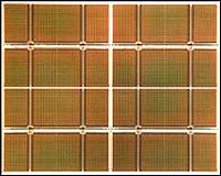
Livermore - Feb 12, 2003 The Federal Laboratory Consortium for Technology Transfer has granted the Extreme Ultraviolet Lithography (EUVL) project an Excellency in Technology Transfer award for technology that will lead to microprocessors that are tens of times faster than today's most powerful chips. The technology also will create memory chips with similar increases in storage capacity. The EUVL team is made up of scientists and researchers from the Lawrence Livermore National Laboratory, Lawrence Berkeley National Laboratory and Sandia National Laboratories collaborating as the Virtual National Laboratory. The team has successfully transferred the EUVL technology under a multi-year CRADA (Cooperative Research and Development Agreement) to the Extreme Ultraviolet Limited Liability Company (EUV LLC), a consortium headed by Intel Corporation that includes chipmakers Advanced Micro Devices, IBM, Infineon, Micron Technologies and Motorola. Current lithography technology -- which uses light, focused by lenses, to imprint features etched on a silicon chip -- has advanced during the past 25 years to essentially double the number of features that can be packed onto each chip every two years. However, by 2007, the steady reduction in feature sizes possible with visible and ultraviolet--light lithography are expected to reach a physical limit, halting advances in the speed and power of microprocessors. EUVL has been targeted by industry as the next-generation lithography approach to be introduced in 2007 for high-volume manufacturing. It uses EUV light with a wavelength 10 times shorter than the current wavelengths. Since the shorter wavelength is absorbed by lenses, the EUVL system must use a reflective optical system (coated mirrors) instead of transmitting lenses for the operating wavelength of 134 Angstroms. Industry watchers say EUV lithography could be used for the next decade, contrasting current lithographic techniques that are typically oudated within a few years. The first full-scale prototype EUVL machine, located at Sandia National Laboratories in Livermore, Calif., was completed in 2001. The technology demonstrated by the prototype machine will make possible microprocessors that are 10 times faster with 10 times as many active transistors and memory chips that can store 40 times more information. "This recognition marks another milestone in the evolution of EUVL technology," said Don Sweeney, Livermore's EUVL program manager and director of the EUV Virtual National Laboratory. "It truly is an honor to be recognized for the successful transfer of fundamental science developed at the national laboratory level to the private sector." The FLC award is only given to organizations that have successfully transferred a technology to a commercial company. A panel of technology transfer experts from industry, state and local government, academia and the federal laboratory system evaluated the nominations. The Lawrence Livermore National Laboratory's EUVL team is headed by Sweeney of the Physics and Advanced Technologies Directorate. Current team members include Jennifer Alameda, Sasa Bajt, Anton Barty, Sherry Baker, Butch Bradsher, Henry Chapman, Carl Chung, Al Edge, Jim Folta, Layton Hale, Stefan Hau-Riege, Michael Johnson, Patrick Kearney, Cindy Larson, Rick Levesque, Paul Mirkarimi, Nhan Nguyen, Gary Otani, Don Phillion, Jeff Robinson, Mark Schmidt, Frank Snell, Gary Sommargren, Regina Soufli, Victor Sperry, Eberhard Spiller, John S. Taylor and Chris Walton. Community Email This Article Comment On This Article Related Links Lawrence Livermore National Laboratory SpaceDaily Search SpaceDaily Subscribe To SpaceDaily Express Space Technology News - Applications and Research
 Baltimore MD (SPX) Jan 12, 2006
A team comprised of three leading US aerospace and defense contractors has demonstrated an innovative technological use of active electronically scanned array (AESA) radars for high-bandwidth communications. |
|
| The content herein, unless otherwise known to be public domain, are Copyright 1995-2006 - SpaceDaily.AFP and UPI Wire Stories are copyright Agence France-Presse and United Press International. ESA PortalReports are copyright European Space Agency. All NASA sourced material is public domain. Additionalcopyrights may apply in whole or part to other bona fide parties. Advertising does not imply endorsement,agreement or approval of any opinions, statements or information provided by SpaceDaily on any Web page published or hosted by SpaceDaily. Privacy Statement |