|
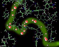
Warwick - Apr 07, 2004 A new generation of materials inspired by the ancient Greeks have been developed by scientists for use in miniaturised devices. The materials are robust, flexible films with perforations on the nano scale and have nano coatings. They are environmentally safe and will enable ultra-fast optoelectronic communication. They are produced by the self-assembly of an intricate 3D jigsaw which is then filled with solid metal or active plastic using the same technology used for plating jewellery. This new technique has been inspired by the lost-wax casting process used by the ancient Greeks for sculpture, but scaled down by a factor of one million. This new technology was described by Professor Jeremy Baumberg in the Mott Lecture on Monday 5th April at the Institute of Physics conference CMMP 2004. This four-day conference is being held this week at the University of Warwick. Professor Baumberg, from Southampton University, said: "These environmentally friendly nano-coatings stay embedded within their operating devices. The nano-perforations produce new electronic, magnetic, optical and bio-sensing properties, applicable to a vast range of new nano-devices in consumer electronics. The complicated 3D nanostructures are impossible to create using conventional micro-technologies, and fill a gap in our ability to build what we need on the nanoscale. He continued: "Our goal is to allow researchers waking up with a smart idea, to design their new nano-device after breakfast, rapidly nano-prototype it after lunch, and to be testing its nano-performance the same evening. Only in this way will we unlock the full creative potential of our innovative researchers, and find the right ways through the vast maze of possible nano-devices". Carefully crafted nano-sized holes in the films also act as pockets for other useful Nano-particles, tethering them in place ("Contained Nano"). The nano-honeycomb structures can provide the equivalent of a scaffolding to assemble nano-devices or sensitive nano-sensors on ultra-small scales. The ultra-high surface area of the nano-films leads to hugely-superior catalytic properties � this is currently being exploited to make cheap greenhouse gas sensors. Growing magnets inside these nano-honeycombs produces nano-materials whose magnetic properties can be adapted for new generations of magnetic memories on a chip. The nano-scaffolds are being investigated for assembling 3D electronic circuits, and to produce 'super-capacitors' for mobile devices. Similarly the nano-films possess new types of structural colour (such as red- or blue-coloured gold) which are environmentally-safe ways of ornamenting surfaces, as well as enabling new devices for fast optoelectronic communication. Community Email This Article Comment On This Article Related Links Institute of Physics SpaceDaily Search SpaceDaily Subscribe To SpaceDaily Express Nano Technology News From SpaceMart.com Computer Chip Architecture, Technology and Manufacture
 New York (UPI) Mar 18, 2005
One of the single biggest applications of nanotechnology could be solving the global shortage of pure water, experts told UPI's Nano World. |
|
| The content herein, unless otherwise known to be public domain, are Copyright 1995-2006 - SpaceDaily.AFP and UPI Wire Stories are copyright Agence France-Presse and United Press International. ESA PortalReports are copyright European Space Agency. All NASA sourced material is public domain. Additionalcopyrights may apply in whole or part to other bona fide parties. Advertising does not imply endorsement,agreement or approval of any opinions, statements or information provided by SpaceDaily on any Web page published or hosted by SpaceDaily. Privacy Statement |