|
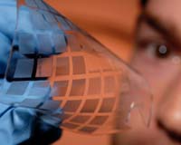
Atlanta GA (SPX) Apr 26, 2006 Using a combination of experimental data and simulations, researchers have identified key parameters that predict the outcome of nanoimprint lithography, a fabrication technique that offers an alternative to traditional lithography in patterning integrated circuits and other small-scale structures into polymers. Results of the three-year study, conducted by researchers at the Georgia Institute of Technology and Sandia National Laboratories, provide a "road map" to guide development of next-generation micron- and nanometer scale high-resolution imprint manufacturing. By reducing cost and time, the design rules could help make high-volume production of nanotechnology-based products more economically feasible. "This work provides a rational link between what engineers want to make using nanoimprint lithography and the path for creating them," said William King, an assistant professor in Georgia Tech's School of Mechanical Engineering. "We have developed manufacturing design rules that will give future users of this technology a predictive tool kit so they'll know what to expect over a broad range of parameters." The research results have been published in the Journal of Vacuum Science Technology B and the Journal of Micromechanics and Microengineering. The research was supported by awards for King through the National Science Foundation's CAREER program and the PECASE award program of the U.S. Department of Energy. Nanoimprint lithography is the ultra-miniaturized version of the decades-old embossing process in which a master tool � or a mold � is pressed into a soft material to create detailed patterns. Using a broad range of polymer materials, nanoimprint lithography produces structures on the micron or nanometer size scales, offering the potential for lowering production costs. However, quality issues caused by unpredictable polymer flow into the non-uniform features of embossing tools pose a major stumbling block. Earlier research into this complex process has produced often conflicting recommendations, forcing manufacturers to pursue costly trial and error. Using the results of experimental work and a simulation program adapted in collaboration with researchers at Sandia National Laboratories, King's research team examined every variable involved in the nanoimprinting process, recording the outcome of each incremental change through the design space. They studied such variables as shear deformation of the polymer, elastic stress release, capillary flow and viscous flow during the filling of imprinting tool cavities that had varying sizes and shapes. "This helped us to resolve the phenomenological events that occur during the manufacturing process and to link them to the observed experimental outcomes," King explained. "Because we have blanketed the entire design space, we have a firm understanding on the linkage between process parameters and outcomes." At the micron- and nanometer size scales studied by the researchers, the fundamental laws of physics remain the same as at larger scales, but manifest themselves in different ways. "At the small scale with embossing and nano-imprinting, different issues are important," King said. "For instance, we can have gradients in surface tension that are very important to how polymer nanostructures are formed. We can also have high pressure gradients inside our embossing tools that are almost ridiculously high compared to what you would expect at the macro scale." The research examined, for example, how large differences in cavity sizes on the imprinting tool lead to non-uniform filling and non-local polymer flow. It also provided recommendations on how to minimize such issues. The research ultimately pointed to specific parameters that determine the outcome of the process. These include key geometric parameters that predict the polymer deformation mechanism. The research also developed a new non-dimensional measure, the "Nanoimprint Capillary Number," which predicts the flow driving mechanism that ultimately governs all of the polymer flow details. By reducing the complex set of variables to key parameters, King � along with Georgia Tech graduate student Harry D. Rowland and collaborators Amy C. Sun and P. Randall Schunk of Sandia National Laboratories � have been able to account for the varying process outcomes reported by other researchers in dozens of papers, King said. The results apply to any polymeric material that follows standard viscous flow rules and produces feature sizes larger than 50 nanometers. The next step in the research would be to modify the simulation software to account for physics changes that occur on smaller size scales. The results could have applications in semiconductor manufacturing, where nanoimprinting offers a potential alternative to increasingly expensive lithography processes to produce circuitry. It could also help make high-volume production of nanoscale structures for optoelectronic, biomedical and other applications more economically feasible. "Nanoscale products are too expensive to manufacture, and they will continue to be too expensive until something fundamentally changes in the process," King added. "Nanotechnology will not be successful until you can go into a grocery store or discount store and routinely purchase products based on nanotechnology. That's what we want to accomplish." Community Email This Article Comment On This Article Related Links Georgia Institute of Technology Computer Chip Architecture, Technology and Manufacture Nano Technology News From SpaceMart.com
 Tampa FL (SPX) Apr 10, 2006
Using the power of modern computing combined with innovative theoretical tools, an international team of researchers has determined how a one-way electrical valve, or diode, made of only a single molecule does its job. Diodes are critical components within computer, audio equipment and countless other electronic devices. |
|
| The content herein, unless otherwise known to be public domain, are Copyright 1995-2006 - SpaceDaily.AFP and UPI Wire Stories are copyright Agence France-Presse and United Press International. ESA PortalReports are copyright European Space Agency. All NASA sourced material is public domain. Additionalcopyrights may apply in whole or part to other bona fide parties. Advertising does not imply endorsement,agreement or approval of any opinions, statements or information provided by SpaceDaily on any Web page published or hosted by SpaceDaily. Privacy Statement |