|
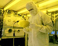
Washington - Mar 16, 2004 A warm winter coat doesn't work nearly as well if it's full of holes. The same is true for hafnium oxide, a promising insulator for the next generation of smaller, faster microchips. While hafnium oxide prevents currents from leaking through the ultrathin layers of semiconductor chips more than 1,000 times better than conventional silicon oxide, its prospects have been dampened by too many current-draining defects. Now a team of National Institute of Standards and Technology (NIST) and IBM researchers reports in the March edition of Electron Device Letters that they have quantified these "electrical capture defects" in a way that may help chipmakers reduce the defects or at least devise a way around them. NIST researcher John S. Suehle called the team's measurements a "critical first step" for improving manufacturing processes. Using a method called "charge pumping," the NIST and IBM scientists found where the defects occur near the interface between the silicon substrate and the hafnium oxide and how those locations are ultimately detrimental to transistor operation. The method involves applying a voltage pulse and then measuring the current coming from a transistor. By changing the characteristics of the voltage pulse used, the scientists were able to measure the electrical-capture capacity of the defects. Community Email This Article Comment On This Article Related Links National Institute of Standards and Technology SpaceDaily Search SpaceDaily Subscribe To SpaceDaily Express Space Technology News - Applications and Research
 Baltimore MD (SPX) Jan 12, 2006
A team comprised of three leading US aerospace and defense contractors has demonstrated an innovative technological use of active electronically scanned array (AESA) radars for high-bandwidth communications. |
|
| The content herein, unless otherwise known to be public domain, are Copyright 1995-2006 - SpaceDaily.AFP and UPI Wire Stories are copyright Agence France-Presse and United Press International. ESA PortalReports are copyright European Space Agency. All NASA sourced material is public domain. Additionalcopyrights may apply in whole or part to other bona fide parties. Advertising does not imply endorsement,agreement or approval of any opinions, statements or information provided by SpaceDaily on any Web page published or hosted by SpaceDaily. Privacy Statement |