|
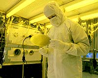
Boston MA (SPX) Jul 22, 2004 In a breakthrough that could lead to dramatically smaller memory chips and other electronic components, Princeton scientists have found a way to mass produce devices that are so small they are at the limit of what can be viewed by the most powerful microscopes. The achievement is an advance over current techniques, which require expensive and time-consuming procedures to create anything so small. The technique offers a relatively simple, low-cost production method that may lead to greater memory capacity and lower costs for computers, digital cameras and other devices. In addition, the scientists achieved unprecedented success in packing the minute structures into dense clusters. The researchers, led by engineering professors Stephen Chou and Stephen Lyon, used a technique known as nanoimprinting, in which they press a mold into a layer of softened plastic on a silicon wafer, making microscopic patterns on the surface of the plastic. The patterns can then be transferred to the silicon where they could form the basis of miniature electronic circuits that store digital information. The goal of the research was to determine how small and dense a pattern could be pressed into plastic with nanoimprinting, said Chou, who invented nanoimprinting in 1994. "This work really pushes the limit down to a few molecules in size," he said. The scientists published their results in the June 28 issue of Applied Physics Letters. The other authors of the paper include graduate students Michael Austin, Wei Wu, Mingtao Li and Zhaoning Yu and postdoctoral researchers Haixiong Ge and Daniel Wasserman. The researchers reported that they created tall, thin ridges only 5 nanometers (5 millionths of a millimeter) wide. The researchers believe they made ridges even narrower than 5 nanometers, but could not confirm the results with existing microscopes. "So we still do not know what the absolute limit is," said Chou. An important aspect of the achievement is not just the small size of the ridges, but also the amount of space between the ridges, Chou said. The spacing, known as "pitch," ultimately determines the density of electronic memory that can be packed onto a chip. In their published paper, the scientists reported that they achieved a 14-nanometer pitch between ridges. They have since reduced it to 12 nanometers. That spacing is a 20-fold reduction compared to the state-of-the-art techniques used in making today's most advanced computer chips and would result in 400 times more memory in a two-dimensional memory chip, Chou said. The current method for making nanoscale devices is to carve each piece individually with a beam of electrons, a technique called electron-beam lithography. That process does not achieve the 14-nanometer pitch of nanoimprinting and requires equipment that is much more expensive than anything used in Chou's technique. The key to the result was the collaboration between the labs of Chou and Lyon and the combination of their different areas of expertise. Chou, the pioneer of nanoimprinting, was looking for improvements in the molds he uses for pressing patterns into plastics. His standard method for making a mold was to use electron-beam lithography to carve the desired pattern in a piece of silicon, which is then pressed into plastic. This approach is limited by the narrowness of the electron beam, which carves out a U-shaped channel about 20 nanometers wide. To improve on this level of precision, Chou turned to Lyon, an expert in a technology called molecular-beam epitaxy, which Lyon uses to grow flat sheets of crystals just a few molecules thick. Members of Lyon's lab grew alternating layers of two materials until they had a wafer hundreds of layers thick. Researchers in Chou's lab then cut the wafer, exposing the edges of the layers. They applied a chemical that ate away one of the two materials but not the other. The result was a very fine comb-like pattern in which all the teeth and valleys were perfectly smooth and square with atomic precision. The researchers used this creation as their mold. This mold-making process, though time-consuming, would need to be done only once in setting up a manufacturing process, said Chou. Once the mold is made, it can be used to make countless copies very rapidly. The research is the latest in a series of nanoimprinting advances Chou has made in recent years. In 2003, Technology Review magazine, published by the Massachusetts Institute of Technology, identified Chou's work with nanoimprinting as one of "10 emerging technologies that will change the world." His latest study was funded in part by the Department of Defense Advanced Research Projects Administration. Community Email This Article Comment On This Article Related Links Princeton University DARPA SpaceDaily Search SpaceDaily Subscribe To SpaceDaily Express Space Technology News - Applications and Research
 Baltimore MD (SPX) Jan 12, 2006
A team comprised of three leading US aerospace and defense contractors has demonstrated an innovative technological use of active electronically scanned array (AESA) radars for high-bandwidth communications. |
|
| The content herein, unless otherwise known to be public domain, are Copyright 1995-2006 - SpaceDaily.AFP and UPI Wire Stories are copyright Agence France-Presse and United Press International. ESA PortalReports are copyright European Space Agency. All NASA sourced material is public domain. Additionalcopyrights may apply in whole or part to other bona fide parties. Advertising does not imply endorsement,agreement or approval of any opinions, statements or information provided by SpaceDaily on any Web page published or hosted by SpaceDaily. Privacy Statement |