|
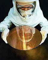
Brussels - Nov 27, 2003 Despite continuous technical advances in the semiconductor industry, microchips are still composed of laterally-arranged (side-by-side) transistors on a silicon substrate. EUREKA project E! 2259 VSI developed new ways to break through this two dimensional approach and the restrictions it imposes by designing 3-D chips or Vertical System Integration (VSI). This technology has immediate security benefits which are very desirable since chip cards often contain secure information or monetary values and, therefore, are subject to attack by hackers. "With the new technology, the top sides of the chips are inside the 3-D stack and therefore not accessible to mechanical attacks, electrical probing or a lot of other physical attacks," says Wolfgang Gruber of Infineon Technologies AG, the German lead partner. Infineon appreciates the co-operation a EUREKA project brings. "EUREKA helped us to find an equipment manufacturer with the necessary know how and skills that are only available in a few companies around the world," explains Gruber. "The EUREKA label is a quality label most people associate with a sophisticated research project of high quality � a big advantage when it comes to convincing someone about your ideas!"
Increased flexibility The Austrian partner Datacon developed the machinery to construct the 3-D chips. "Through our close co-operation with Infineon we were able to produce a machine that could exceed the state-of-the-art in terms of production speed and accuracy," says Christoph Scheiring, Manager of Advanced Technology at Datacon. The partners have developed two versions of the 3-D stacking. The first will be ready for production in 2004, and is "a cost-efficient, two-layer technology called 'Solid Face to Face' (F2F), in which one or more chips are attached and in contact with a base chip by a soldering process." Gruber explains, "a demonstration chip card with a huge amount of memory capable of fulfilling requirements for future multi-application operating systems has been built." Work continues on the second version - a multi-layer technology based on F2F that will allow for wiring through a chip to the next chip, thus making stacks of three or more layers possible and further increasing the chip's flexibility and security. This is due to be ready for production in 2007. Community Email This Article Comment On This Article Related Links EUREKA Be SpaceDaily Search SpaceDaily Subscribe To SpaceDaily Express Space Technology News - Applications and Research
 Baltimore MD (SPX) Jan 12, 2006
A team comprised of three leading US aerospace and defense contractors has demonstrated an innovative technological use of active electronically scanned array (AESA) radars for high-bandwidth communications. |
|
| The content herein, unless otherwise known to be public domain, are Copyright 1995-2006 - SpaceDaily.AFP and UPI Wire Stories are copyright Agence France-Presse and United Press International. ESA PortalReports are copyright European Space Agency. All NASA sourced material is public domain. Additionalcopyrights may apply in whole or part to other bona fide parties. Advertising does not imply endorsement,agreement or approval of any opinions, statements or information provided by SpaceDaily on any Web page published or hosted by SpaceDaily. Privacy Statement |