|
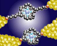
Durham NC (SPX) Aug 02, 2007 In an assist in the quest for ever smaller electronic devices, Duke University engineers have adapted a decades-old computer aided design and manufacturing process to reproduce nanosize structures with features on the order of single molecules. The new automated technique for nanomanufacturing suggests that the emerging nanotechnology industry might capitalize on skills already mastered by today's engineering workforce, according to the researchers. "These tools allow you to go from basic, one-off scientific demonstrations of what can be done at the nanoscale to repetitively engineering surface features at the nanoscale," said Rob Clark, Thomas Lord Professor and chair of the mechanical engineering and materials science department at Duke University's Pratt School of Engineering. The feat was accomplished by using the traditional computing language of macroscale milling machines to guide an atomic force microscope (AFM). The system reliably produced 3-D, nanometer-scale silicon oxide nanostructures through a process called anodization nanolithography, in which oxides are built on semiconducting and metallic surfaces by applying an electric field in the presence of tiny amounts of water. "That's the key to moving from basic science to industrial automation," Clark said. "When you manufacture, it doesn't matter if you can do it once, the question is: Can you do it 100 million times and what's the variability over those 100 million times" Is it consistent enough that you can actually put it into a process"" Clark and Matthew Johannes, who recently received his doctoral degree at Duke, will report their findings in the August 29 issue of the journal Nanotechnology (now available online) and expect to make their software and designs freely available online. The work was supported by the National Science Foundation. Atomic force microscopes (AFMs), which can both produce images and manipulate individual atoms and molecules, have been the instrument of choice for researchers creating localized, two-dimensional patterns on metals and semiconductors at the nanoscale. Yet those nanopatterning systems have relied on the discrete points of a two-dimensional image for laying out the design. "Now we've added another dimension," Johannes said. The researchers showed they could visualize 3-D structures-including a series of squares that differed in size, and a star--in a computerized design environment and then automatically build them at the nanoscale. The structures they produced were measured in nanometers-one billionth of a meter-about 80,000 times smaller than the diameter of a human hair. Johannes had to learn to carefully control the process by adjustments to the humidity, voltage, and scanning speed, relying on sensors to guide the otherwise invisible process. The new technique suggests that the nanotechnology factories of the future might not operate so differently from existing manufacturing plants. "If you can take prototyping and nanomanufacturing to a level that leverages what engineers know how to do, then you are ahead of the game," Clark said. "Most engineers with conventional training don't think about nanoscale manipulation. But if you want to leverage a workforce that's already in place, how do you set up the future of manufacturing in a language that engineers already use to communicate" That's what we're focused on doing here." Community Email This Article Comment On This Article Related Links Duke University Nano Technology News From SpaceMart.com Computer Chip Architecture, Technology and Manufacture
 Washington DC (SPX) Jul 31, 2007
The Environmental Protection Agency (EPA) must make key decisions about how to apply the two major end-of-life statutes to nanotechnology waste in order to ensure adequate oversight for these technologies, concludes a new report from the Wilson Center's Project on Emerging Nanotechnologies. However, the report notes that the Agency lacks much of the data on human health and eco-toxicity that form the basis for such determinations, creating some tough challenges ahead in EPA's decision-making process. |
|
| The content herein, unless otherwise known to be public domain, are Copyright 1995-2007 - SpaceDaily.AFP and UPI Wire Stories are copyright Agence France-Presse and United Press International. ESA Portal Reports are copyright European Space Agency. All NASA sourced material is public domain. Additional copyrights may apply in whole or part to other bona fide parties. Advertising does not imply endorsement,agreement or approval of any opinions, statements or information provided by SpaceDaily on any Web page published or hosted by SpaceDaily. Privacy Statement |