|
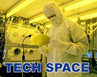
Evanston IL (SPX) Sep 28, 2004 Silicon microelectronics has undergone relentless miniaturization during the past 30 years, leading to dramatic improvements in computational capacity and speed. But the end of that road is fast approaching, and scientists and engineers have been investigating another promising avenue: using individual molecules as functional electronic devices. Now a team of engineers at Northwestern University has become the first to precisely align multiple types of molecules on a silicon surface at room temperature - an important step toward the goal of molecular electronics. The results, which demonstrate patterning on a scale 10,000 times smaller than that of microelectronics, were published Sept. 27 as the cover story of the journal Applied Physics Letters (APL). "We have demonstrated a strategy for intentionally positioning molecules, which is necessary for the construction of nanoscale systems such as molecular transistors or light-emitting diodes," said Mark C. Hersam, assistant professor of materials science and engineering, who led the research team. "Our process works at room temperature and on silicon, which suggests that it can be made compatible with conventional silicon microelectronics. Ultimately, we want to integrate with current technology, thus creating a bridge between microelectronics and nanoelectronics." The nanofabrication process, called multi-step feedback-controlled lithography, is useful for a variety of fundamental studies and for the construction and testing of prototype nanoscale devices that could be used in future technologies ranging from consumer electronics to biomedical diagnostics. "Previously we were working with single molecules on silicon," said Hersam. "This new process enables us to build more complex structures. Plus, the technique is general and can be used with many different molecules, which increases its potential." The researchers demonstrated their process using a custom-built ultrahigh-vacuum scanning tunneling microscope. With this tool, they constructed chains consisting of styrene and a molecule known as TEMPO and now are studying the electronic properties of this novel nanostructure. Community Email This Article Comment On This Article Related Links Northwestern University SpaceDaily Search SpaceDaily Subscribe To SpaceDaily Express Space Technology News - Applications and Research
 Baltimore MD (SPX) Jan 12, 2006
A team comprised of three leading US aerospace and defense contractors has demonstrated an innovative technological use of active electronically scanned array (AESA) radars for high-bandwidth communications. |
|
| The content herein, unless otherwise known to be public domain, are Copyright 1995-2006 - SpaceDaily.AFP and UPI Wire Stories are copyright Agence France-Presse and United Press International. ESA PortalReports are copyright European Space Agency. All NASA sourced material is public domain. Additionalcopyrights may apply in whole or part to other bona fide parties. Advertising does not imply endorsement,agreement or approval of any opinions, statements or information provided by SpaceDaily on any Web page published or hosted by SpaceDaily. Privacy Statement |