|
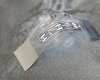
Washington DC (SPX) Sep 14, 2005 Although still in the qualifying rounds, U.S. researchers are helping manufacturers win the race to develop low-cost ways to commercialize a multitude of products based on inexpensive organic electronic materials - from large solar-power arrays to electronic newspapers that can be bent and folded. In the on-line issue of Advanced Materials,* researchers from the National Institute of Standards and Technology (NIST) and the University of California at Berkeley report success in using a non-destructive measurement method to detail three structural properties crucial to making reliable electronic devices with thin films of the carbon-rich (organic) semiconductors. The new capability could help industry clear hurdles responsible for high manufacturing development costs that stand in the way of widespread commercial application of the materials. With the technique called near-edge X-ray absorption fine-structure spectroscopy, or NEXAFS, the team tracked chemical reactions, molecular reordering and defect formation over a range of processing temperatures. They then evaluated how process-induced changes in thin-film composition and structure affected the movement of charge carriers (either electrons or electron "holes") in organic field effect transistors, devices basic to electronic circuits. With NEXAFS measurements taken over the range from room temperature to 300 degrees Celsius, the team monitored the conversion of a precursor chemical to an oligothiophene, an organic semiconductor. The molecular organization and composition achieved at 250 degrees Celsius yielded the highest levels of charge carrier movement and, consequently, maximum electric-current flow. As chemical conversion progressed, the researchers calculated how the molecules arranged themselves on top of an electrical insulator. Top transistor performance corresponded to a vertical alignment of molecules. In addition, they used NEXAFS to determine the angles of chemical bonds and to assess the thickness and uniformity of film coverage, also critical to performance. NEXAFS has the potential to be the "ideal measurement platform for systematic investigation" of organic electronic materials, says lead investigator Dean DeLongchamp, a NIST materials scientist. "A straightforward means of correlating chemical and physical structure to the electronic performance of organic semiconductor films is a much-needed tool." *D.M. DeLongchamp, S. Sambasivan, D.A. Fischer, E.K. Lin, P. Chang, A.R. Murphy, J.M.J. Frechet, and V. Subramanian, "Direct Correlation of Organic semiconductor film structure to field-effect mobility," Advanced Materials, published online Aug. 30, 2005, DOI number (10.1002/adma.200500253). Community Email This Article Comment On This Article Related Links National Institute of Standards and Technology SpaceDaily Search SpaceDaily Subscribe To SpaceDaily Express Computer Chip Architecture, Technology and Manufacture Nano Technology News From SpaceMart.com
 Chicago (UPI) Oct 7, 2005
Chips that track boxes on trucks and ships soon may be sophisticated enough to monitor every move of consumers, a controversial new book claims. |
|
| The content herein, unless otherwise known to be public domain, are Copyright 1995-2006 - SpaceDaily.AFP and UPI Wire Stories are copyright Agence France-Presse and United Press International. ESA PortalReports are copyright European Space Agency. All NASA sourced material is public domain. Additionalcopyrights may apply in whole or part to other bona fide parties. Advertising does not imply endorsement,agreement or approval of any opinions, statements or information provided by SpaceDaily on any Web page published or hosted by SpaceDaily. Privacy Statement |